


Dongguan Phynam Comtech Co.,Limited
Features
Commercial : -5 to +70℃
Extended: -20~80℃
Industrial : -40 to +85℃
Applications
Description
HD-SFP+/10G-LR 10Gb/s SFP+ transceivers are designed for use in 10-Gigabit Ethernet links up to 20km over Single Mode fiber.
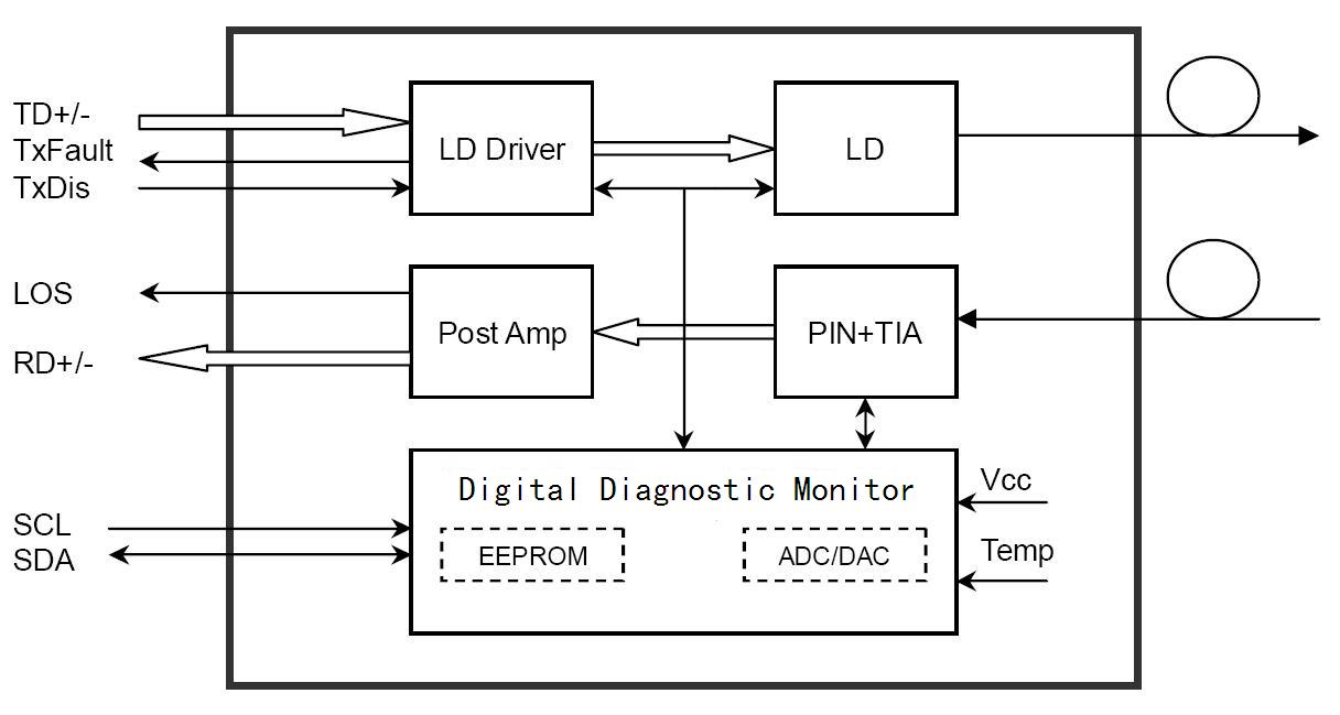
Module Block Diagram
Absolute Maximum Ratings
|
Parameter |
Symbol |
Min. |
Typical |
Max. |
Unit |
|
|
Power Supply Voltage |
VCC |
0 |
3.6 |
V |
||
|
Storage Temperature |
Ts |
-40 |
+85 |
C |
||
|
Operating Case Temperature |
Commercial |
Tc |
-5 |
+70 |
°C |
|
|
Extended |
-20 |
+80 |
°C |
|||
|
Industrial |
-40 |
+85 |
°C |
|||
|
Relative Humidity |
RH |
0 |
85 |
% |
||
|
RX Input Average Power |
Pmax |
- |
0 |
dBm |
||
Recommended Operating Environment:
|
Parameter |
Symbol |
Min. |
Typical |
Max. |
Unit |
|
Power Supply Voltage |
VCC |
3.135 |
3.3 |
3.465 |
V |
|
Power Supply Current |
Icc |
300 |
mA |
||
|
Operating Case Temperature |
TC |
-40 |
85 |
C |
|
|
Bit Rate |
BR |
9.953 10GBASE-LW |
Gb/s |
||
|
10.3125 10GBASE-LR |
|||||
|
8.5 800-SM-LC-L |
|||||
|
10.51875 1200-SM-LL-L |
|||||
Electrical Characteristics
|
Parameter |
Symbol |
Min. |
Typical |
Max. |
Unit |
Note |
|
Supply Voltage |
Vcc |
3.0 |
3.30 |
3.60 |
V |
|
|
Supply Current |
Icc |
160 |
280 |
mA |
||
|
Transmitter Section: |
||||||
|
Input differential impedance |
Rin |
90 |
100 |
110 |
|
|
|
Single ended data input swing |
Vin PP |
180 |
700 |
mVp-p |
||
|
Transmit Disable Voltage |
VD |
Vcc – 1.3 |
Vcc |
V |
||
|
Transmit Enable Voltage |
VEN |
Vee |
Vee+ 0.8 |
V |
||
|
Receiver Section: |
||||||
|
Single ended data output swing |
Vout,pp |
300 |
850 |
mv |
2,6 |
|
|
Data output rise time |
tr |
ps |
3 |
|||
|
Data output fall time |
tf |
ps |
3 |
|||
|
LOS Fault |
Vlosfault |
Vcc – 0.5 |
VCC_host |
V |
4 |
|
|
LOS Normal |
Vlos norm |
Vee |
Vee+0.5 |
V |
4 |
|
Notes:
1. Connected directly to TX data input pins. AC coupling from pins into laser driver IC.
2. Into 100Ω differential termination.
3. 20 – 80%. Measured with Module Compliance Test Board and OMA test pattern. Use of four 1’s and four 0’s sequence in the PRBS 9 is an acceptable alternative. SFF-8431 Rev 4.1.
4. LOS is an open collector output. Should be pulled up with 4.7kΩ – 10kΩ on the host board. Normal operation is logic 0; loss of signal is logic 1.
5. See Section 2.8.3 of SFF-8431 Rev 4.1
Optical Parameters
|
Parameter |
Symbol |
Min. |
Typical |
Max. |
Unit |
Note |
|
Transmitter Section: |
||||||
|
Center Wavelength |
λt |
1260 |
1310 |
1355 |
nm |
|
|
Side Mode Suppression Ratio |
SMSR |
30 |
- |
- |
dB |
|
|
Average Optical Power |
Pavg |
-5.0 |
-2.5 |
+1 |
dBm |
|
|
Optical Power OMA |
Poma |
-4.0 |
- |
- |
dBm |
|
|
Laser Off Power |
Poff |
- |
- |
-30 |
dBm |
|
|
Extinction Ratio |
ER |
3.5 |
- |
- |
dB |
|
|
Transmitter Dispersion Penalty |
TDP |
- |
- |
3.2 |
dB |
|
|
Relative Intensity Noise |
Rin |
- |
- |
-128 |
dB/Hz |
12dB reflection |
|
Optical Return Loss Tolerance |
- |
- |
12 |
dB |
||
|
Receiver Section: |
||||||
|
Center Wavelength |
λr |
1260 |
1310 |
1355 |
nm |
|
|
Receiver Sensitivity in Average Power |
Sen |
-14.4 |
dBm |
1 |
||
|
Receiver Sensitivity (OMA) |
Sen-oma |
- |
- |
-12.6 |
dBm |
2 |
|
Stressed Sensitivity (OMA) |
- |
- |
-10.3 |
dBm |
2 |
|
|
Vertical eye closure penalty |
2.2 |
- |
- |
dB |
3 |
|
|
Los Assert |
LosA |
-30 |
- |
- |
dBm |
|
|
Los Dessert |
LosD |
- |
- |
-16 |
dBm |
|
|
Los Hysteresis |
LosH |
0.5 |
- |
- |
dB |
|
|
Overload |
Pin |
- |
- |
0.5 |
dBm |
1 |
|
Receiver Reflectance |
- |
- |
-12 |
dB |
||
|
Stressed eye jitter |
0.3 |
- |
- |
UIp-p |
2 |
|
|
Receive electrical 3dB upper cutoff frequency |
- |
- |
12.3 |
GHz |
||
|
Receiver power (damage) |
- |
- |
1.5 |
dBm |
||
Notes:
Timing Characteristics:
|
Parameter |
Symbol |
Min. |
Typical |
Max. |
Unit |
|
TX_Disable Assert Time |
t_off |
10 |
us |
||
|
TX_Disable Negate Time |
t_on |
1 |
ms |
||
|
Time to Initialize Include Reset of TX_FAULT |
t_int |
300 |
ms |
||
|
TX_FAULT from Fault to Assertion |
t_fault |
100 |
us |
||
|
TX_Disable Time to Start Reset |
t_reset |
10 |
us |
||
|
Receiver Loss of Signal Assert Time |
TA,RX_LOS |
100 |
us |
||
|
Receiver Loss of Signal Deassert Time |
Td,RX_LOS |
100 |
us |
||
|
Rate-Select Change Time |
t_ratesel |
10 |
us |
||
|
Serial ID Clock Time |
t_serial-clock |
100 |
kHz |
Digital Diagnostic Monitor Characteristics
The following digital diagnostic characteristics are defined over the Recommended Operating Environment unless otherwise specified. It is compliant to SFF8472 Rev10.2 with internal calibration mode. For external calibration mode please contact our sales stuff.
|
Parameter |
Symbol |
Min. |
Max. |
Unit |
|
Temperature monitor absolute error |
DMI_Temp |
-3 |
3 |
degC |
|
Laser power monitor absolute error |
DMI_TX |
-3 |
3 |
dB |
|
RX power monitor absolute error |
DMI_RX |
-3 |
3 |
dB |
|
Supply voltage monitor absolute error |
DMI_VCC |
-0.08 |
0.08 |
V |
|
Bias current monitor absolute error |
DMI_Ibias |
-10% |
10% |
mA |
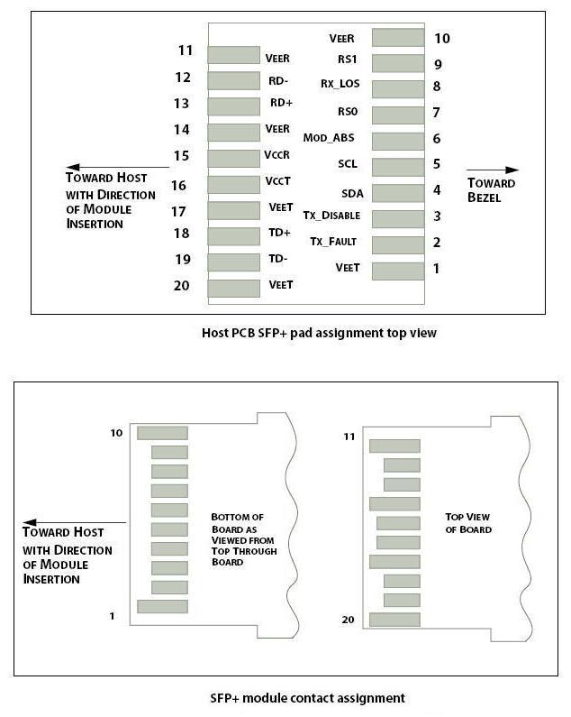
Pin Descriptions
|
PIN |
Logic |
Symbol |
Name / Description |
Note |
|
1 |
VeeT |
Module Transmitter Ground |
1 |
|
|
2 |
LVTTL-O |
TX_Fault |
Module Transmitter Fault |
|
|
3 |
LVTTL-I |
TX_Dis |
Transmitter Disable; Turns off transmitter laser output |
|
|
4 |
LVTTL-I/O |
SDA |
2-Wire Serial Interface Data Line |
2 |
|
5 |
LVTTL-I |
SCL |
2-Wire Serial Interface Clock |
2 |
|
6 |
MOD_DEF0 |
Module Definition, Grounded in the module |
||
|
7 |
LVTTL-I |
RS0 |
Receiver Rate Select |
|
|
8 |
LVTTL-O |
RX_LOS |
Receiver Loss of Signal Indication Active LOW |
|
|
9 |
LVTTL-I |
RS1 |
Transmitter Rate Select (not used) |
|
|
10 |
VeeR |
Module Receiver Ground |
1 |
|
|
11 |
VeeR |
Module Receiver Ground |
1 |
|
|
12 |
CML-O |
RD- |
Receiver Inverted Data Output |
|
|
13 |
CML-O |
RD+ |
Receiver Data Output (not used) |
|
|
14 |
VeeR |
Module Receiver Ground |
1 |
|
|
15 |
VccR |
Module Receiver 3.3 V Supply |
||
|
16 |
VccT |
Module Receiver 3.3 V Supply |
||
|
17 |
VeeT |
Module Transmitter Ground |
1 |
|
|
18 |
CML-I |
TD+ |
Transmitter Non-Inverted Data Input |
|
|
19 |
CML-I |
TD- |
Transmitter Inverted Data Input |
|
|
20 |
VeeT |
Module Transmitter Ground |
1 |
SFP+ Module PIN Definition
Notes:
1. Module ground pins GND are isolated from the module case.
2. Shall be pulled up with 4.7K-10Kohms to a voltage between 3.15V and 3.45V on the host board.
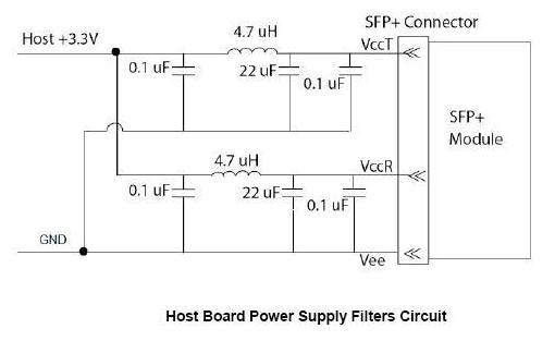
Recommended Power Interface Circuit
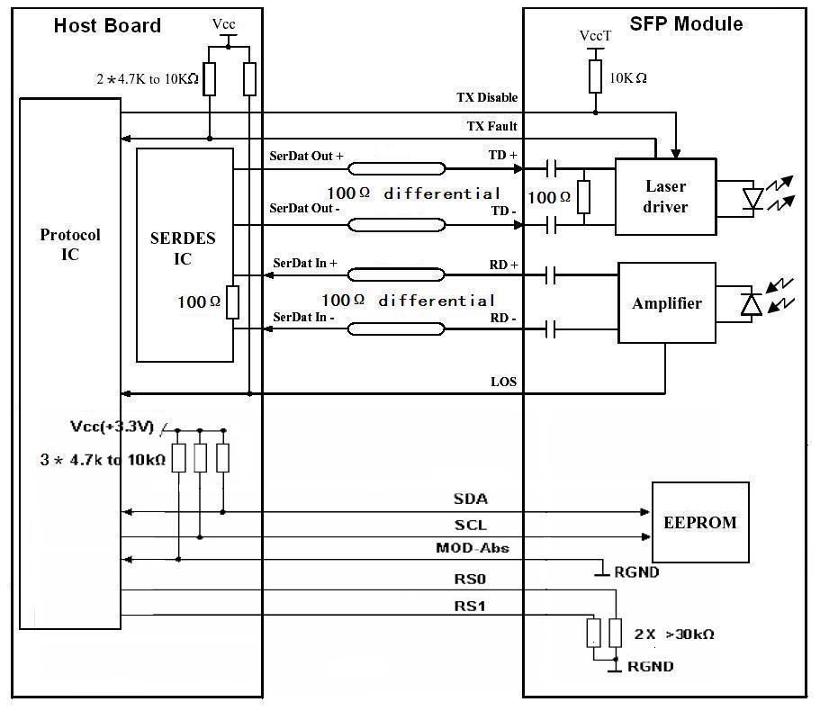
Host - Transceiver Interface Block Diagram
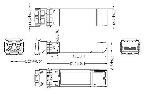
Mechanical Dimensions
Ordering information
|
Part Number |
Product Description |
|
HD-SFP+/10G-LR |
1310nm, 10Gbps, 20Km, SFP+ Transceiver -5ºC ~ +70ºC . |
|
HD-SFP+/10G-LR-E |
1310nm, 10Gbps, 20Km, SFP+ Transceiver -20ºC ~ +80ºC . |
|
HD-SFP+/10G-LR-I |
1310nm, 10Gbps, 20Km, SFP+ Transceiver -40ºC ~ +85ºC . |
References
1. “Specifications for Enhanced Small Form Factor Pluggable Module SFP+”,SFF-8431, Rev 4.1, July 6, 2009.
2. “Improved Pluggable Formfactor”,SFF-8432, Rev 4.2,Apr 18,2007
3. IEEE802.3ae – 2002
4. “Diagnostic Monitoring Interface for Optical Transceivers” SFF-8472, Rev 10.2, June 1, 2007
Performance figures, data and any illustrative material provided in this data sheet are typical and must be specifically confirmed in writing by Handar before they become applicable to any particular order or contract. In accordance with the Handar policy of continuous improvement specifications may change without notice. The publication of information in this data sheet does not imply freedom from patent or other protective rights of Handar or others. Further details are available from any Handar sales representative.
