


Dongguan Phynam Comtech Co.,Limited
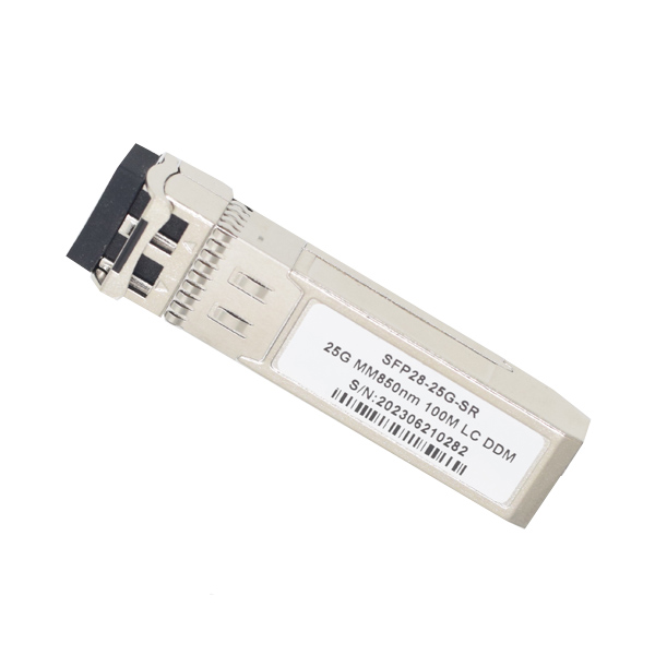
SFP28 Transceiver 850nm 100m over MM DDM
Features
Application
Standard
Specification
|
Absolute Maximum Ratings |
||||
|
Parameter |
Symbol |
Min |
Max |
Unit |
|
Storage temperature |
TS |
-40 |
85 |
℃ |
|
Power Supply Voltage |
Vcc |
0 |
3.6 |
V |
|
Relative Humidity |
RH |
5 |
95 |
% |
|
Recommended Operating Conditions |
|||||
|
Parameter |
Symbol |
Min |
Typical |
Max |
Unit |
|
Operating Case Temperature (Commercial) |
Tc |
0 |
70 |
℃ |
|
|
Power Supply Voltage |
Vcc |
3.13 |
3.3 |
3.47 |
V |
|
Supply Current |
Icc |
300 |
mA |
||
|
Data Rate |
- |
25.78 |
28.05 |
Gbps |
|
|
Fiber Length on 50/125μm high-bandwidth (OM3) MMF |
70 |
m |
|||
|
Fiber Length on 50/125μm high-bandwidth (OM4) MMF |
100 |
m |
|||
|
Optical transmitter Characteristics |
||||||||
|
Parameter |
Symbol |
Min |
Typical |
Max |
Unit |
Notes |
||
|
Launched Power (avg.) |
Pout |
-9.1 |
2.4 |
dBm |
||||
|
Optical Power OMA |
POMA |
-6.4 |
3 |
dBm |
||||
|
Operating Wavelength Range |
λc |
840 |
850 |
860 |
nm |
|||
|
Spectral Width (-20dB) |
σ |
0.6 |
nm |
|||||
|
Extinction Ratio |
ER |
2 |
dB |
|||||
|
Differential data input swing |
VIN,PP |
40 |
1000 |
mV |
||||
|
Input Differential Impedance |
ZIN |
90 |
100 |
110 |
Ω |
|||
|
TX |
Disable |
2.0 |
Vcc |
V |
||||
|
Enable |
0 |
0.8 |
V |
|||||
|
TX |
Fault |
2.0 |
Vcc |
V |
||||
|
Normal |
0 |
0.8 |
V |
|||||
|
Output Eye Diagram |
Complies with IEEE802.3z eye masks when filtered |
|||||||
|
Optical receiver Characteristics |
||||||||
|
Parameter |
Symbol |
Min |
Typical |
Max |
Unit |
Notes |
||
|
Receiver Sensitivity |
S |
-11 |
dBm |
|||||
|
Stressed Sensitivity (OMA) |
- |
- |
-5.2 |
dBm |
||||
|
Wavelength Range |
λc |
840 |
850 |
860 |
nm |
|||
|
Receiver Power (OMA) |
P |
3 |
dBm |
|||||
|
LOS |
Optical De-assert |
Pd |
-13 |
dBm |
||||
|
Optical Assert |
Pa |
-30 |
||||||
|
LOS |
High |
2.0 |
Vcc |
V |
||||
|
Low |
0.8 |
V |
||||||
|
LOS hysteresis |
0.5 |
dB |
||||||
|
Differential data output swing |
Vout,PP |
500 |
1130 |
mV |
||||
|
Timing and Electrical |
|||||
|
Parameter |
Symbol |
Min |
Max |
Unit |
Conditions |
|
Tx-Disable assert time |
T_off |
100 |
us |
Rising edge of Tx_Disable to fall of output signal below 10% of nominal |
|
|
Tx-Disable negate time |
T_on |
2 |
ms |
Falling edge of Tx_Disable to rise of output signal above 90% of nominal,this is only applies in normal operation,ont during start up or fault recorvery. |
|
|
Time to initialize 2-wire interface |
t_2w_start_up |
300 |
ms |
From power on or hot plug after the supply meeting |
|
|
Time to initialize |
T_start_up |
300 |
ms |
From power supplies meeting hot plug or Tx disable negated during power up ,or Tx_Fault recovery,unitl non-cooled power level I part is full operational |
|
|
Time to initialize cooled module and time to power up a cooled module to power level II |
T_start_up_cooled |
90 |
S |
From power supplies meeting hot plug or Tx disable negated during power up ,or Tx_Fault recovery,unitl non-cooled power level I part is full operational.Also,from stoop bit low-to-high SDA transition enabling Power Level II until cooled module is fully operational. |
|
|
Time to Power up to level II |
T_power_level2 |
300 |
ms |
From stop bit low-to-hight SDA transition enabling power Level II until non-cooled module is fully opertational. |
|
|
Time to Power Down from level II |
T_power_down |
300 |
ms |
From stop bit low-to-high SDA transition disabling power level II until module is within power level I requirements. |
|
|
Tx_Fault assert |
Tx_Fault_on |
1 |
ms |
From occurrence of fault to assertion of Tx_Fault. |
|
|
Tx_Fault assert for cooled module |
Tx_Fault_on_cooled |
50 |
ms |
From occurrence of fault to assertion of Tx_Fault. |
|
|
Tx_Fault Reset |
T_reset |
10 |
us |
Time Tx_Disable must be held high to reset Tx_Fault. |
|
|
RSO,RSI rate select timing for FC |
T_RSO_FC,T_RSI_FC |
500 |
us |
From assertion till stable output |
|
|
RSO,RSI rate select timing non FC |
T_RSO,T_RSI |
24 |
ms |
From assertion till stable output |
|
|
Rx_LOS assert delay |
T_los_on |
100 |
us |
From occurrence of loss of signal to assertion of Rx_LOS |
|
|
Rx_LOS assert delay |
T_los_off |
100 |
us |
From occurrence of loss of signal to negation of Rx_LOS |
|
Digital Diagnostic Monitoring Information
|
Parameter |
Accuracy |
Calibration |
Range |
|
Temperature |
±3°C |
internal/ External |
0~70°C |
|
Voltage |
±3% |
internal/ External |
3.0 to 3.6 V |
|
Bias Current |
±10% |
internal/ External |
0 to 20 mA |
|
TX Power |
±3dB |
internal/ External |
-9.1 to 2.4 dBm |
|
RX Power |
±3dB |
internal/ External |
-11 to 0 dBm |
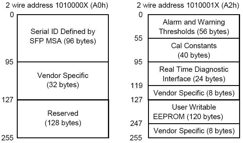
Digital Diagnostic Memory Map
The transceivers provide serial ID memory contents and diagnostic information about the present operating conditions by the 2-wire serial interface (SCL, SDA).
The diagnostic information with internal calibration or external calibration all are implemented, including received power monitoring, transmitted power monitoring, bias current monitoring, supply voltage monitoring and temperature monitoring.
The digital diagnostic memory map specific data field defines as following.
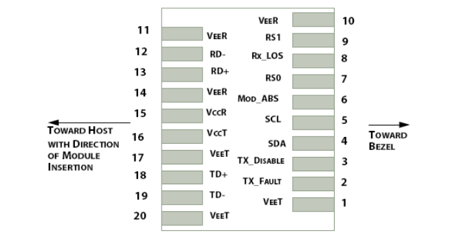
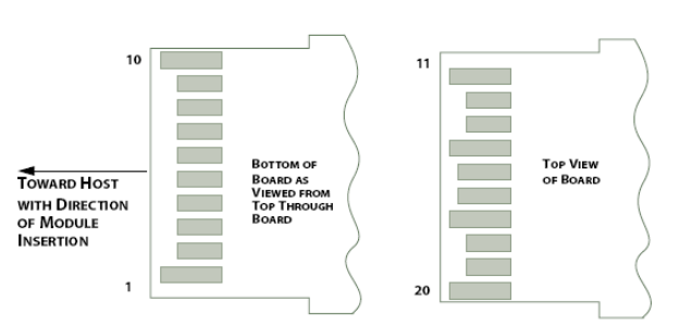
Pin Descriptions
|
Pin |
Name |
Function/Description |
Logic |
Note |
|
1 |
VeeT |
Transmitter Ground |
1 |
|
|
2 |
TX_Fault |
Transmitter Fault |
LVTTL-O |
2 |
|
3 |
TX_Disable |
Transmitter Disable. High: Transmitter off; Low: Transmitter on |
LVTTL-I |
|
|
4 |
SDA |
2-Wire Serial Interface Data Line |
LVTTL-O/I |
2 |
|
5 |
SCL |
2-Wire Serial Interface Clock |
LVTTL-I |
2 |
|
6 |
Mod_ABS |
Module Absent, Connect to VeeT or VeeR in Module |
||
|
7 |
RS0 |
Rate Select 0, optionally controls SFP module receiver |
LVTTL-I |
|
|
8 |
RX_LOS |
Receiver Loss of Signal indication. High: loss of signal; Low: signal detected |
LVTTL-O |
|
|
9 |
RS1 |
Rate Select 1, optionally controls SFP module transmitter |
LVTTL-I |
|
|
10 |
VeeR |
Receiver Ground |
1 |
|
|
11 |
VeeR |
Receiver Ground |
1 |
|
|
12 |
RD- |
Receiver Inverted Data Output |
CML-O |
|
|
13 |
RD+ |
Receiver Data Output |
CML-O |
|
|
14 |
VeeR |
Module Receiver Ground |
1 |
|
|
15 |
VccR |
Receiver Power 3.3V Supply |
||
|
16 |
VccT |
Transmitter Power 3.3V Supply |
||
|
17 |
VeeT |
Module Transmitter Ground |
1 |
|
|
18 |
TD+ |
Transmitter Non-Inverted Data Input |
CML-I |
|
|
19 |
TD- |
Transmitter Inverted Data Input |
CML-I |
|
|
20 |
VeeT |
Module Transmitter Ground |
1 |
Notes:
Shall be pulled up with 4.7K-10Kohms to a voltage between 3.15V and 3.45V on the host board.
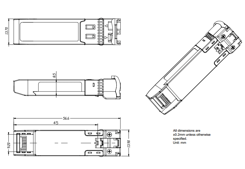
Package Outline
Dimensions are in millimeters. All dimensions are ±0.2mm unless otherwise specified. (Unit: mm)
Regulatory Compliance
|
Feature |
Test |
Method |
|
Electrostatic Discharge (ESD) to the Electrical Pins |
MIL-STD-883E Method 3015.7 |
Class 1 (>1.5kV) – Human Body Model |
|
Electrostatic Discharge (ESD) Immunity |
IEC61000-4-2 |
Class 2(>4.0kV) |
|
Electromagnetic Interference (EMI) |
CISPR22 ITE Class B FCC Class B CENELEC EN55022 VCCI Class 1 |
|
|
Immunity |
IEC61000-4-3 |
Comply with standard |
|
Eye Safety |
FDA 21CFR 1040.10 and 1040.11 EN (IEC) 60825-1,2 |
Compatible with Class I laser Product |
