Dongguan Phynam Comtech Co.,Limited
40G QSFP+ Active Optical Cable
PHQAOC768XX
Features
Applications
Description
The QSFP+ active optic cables are a high performance, low power consumption, long reach interconnect solution supporting InfiniBand QDR/DDR/SDR,12.5G/10G/8G/4G/2G fiber
channel ,PCIe and SAS. It is compliant with the QSFP MSA and IEEE P802.3ba. QSFP AOC is an assembly of 4 full-duplex lanes, where each lane is capable of transmitting data at rates up to 11.3Gb/s, providing an aggregated rate of 45.2Gb/s. QSFP+AOC is one kind of parallel transceiver which provides increased port density and total system cost savings.
Absolute Maximum Ratings
The operation in excess of any absolute maximum ratings might cause permanent damage to this module.
|
Parameter |
Symbol |
Min |
Max |
Unit |
Note |
|
Storage Temperature |
TST |
-40 |
85 |
degC |
|
|
Relative Humidity(non-condensing) |
RH |
0 |
85 |
% |
|
|
Operating Case Temperature |
TOPC |
0 |
70 |
degC |
|
|
Supply Voltage |
VCC |
-0.3 |
3.6 |
V |
|
|
Input Voltage |
Vin |
-0.3 |
Vcc+0.3 |
V |
|
Parameter |
Symbol |
Min |
Typical |
Max |
Unit |
|
Operating Case Temperature |
TOPC |
0 |
70 |
degC |
|
|
Power Supply Voltage |
VCC |
3.13 |
3.3 |
3.47 |
V |
|
Power Consumption |
- |
1.5 |
W |
||
|
Data Rate |
DR |
1 |
10.3 |
11.3 |
Gbps |
|
Data Speed Tolerance |
∆DR |
-100 |
+100 |
ppm |
|
|
Link Distance with OM3 fiber |
D |
0 |
100 |
m |
Recommended Operating Conditions and Supply Requirement
Electrical Specifications
|
Parameter |
Symbol |
Min |
Typical |
Max |
Unit |
|
Differential input impedance |
Zin |
90 |
100 |
110 |
ohm |
|
Differential Output impedance |
Zout |
90 |
100 |
110 |
ohm |
|
Differential input voltage amplitude |
ΔVin |
300 |
1100 |
mVp-p |
|
|
Differential output voltage amplitude |
ΔVout |
500 |
800 |
mVp-p |
|
|
Bit Error Rate |
BR |
E-12 |
|||
|
Input Logic Level High |
VIH |
2.0 |
VCC |
V |
|
|
Input Logic Level Low |
VIL |
0 |
0.8 |
V |
|
|
Output Logic Level High |
VOH |
VCC-0.5 |
VCC |
V |
|
|
Output Logic Level Low |
VOL |
0 |
0.4 |
V |
|
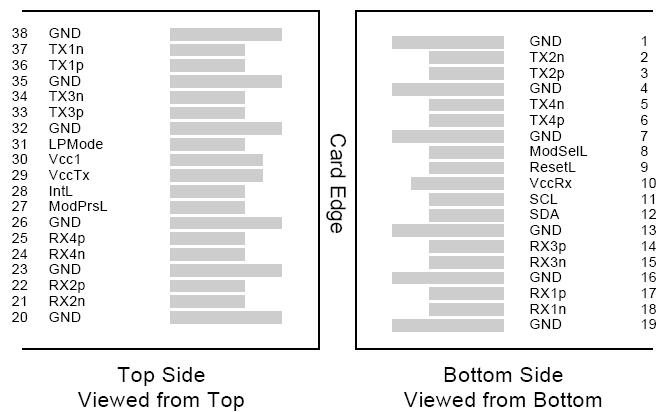
Pin Descriptions
|
PIN |
Logic |
Symbol |
Name/Description |
Note |
|
1 |
GND |
Ground |
1 |
|
|
2 |
CML-I |
Tx2n |
Transmitter Inverted Data Input |
|
|
3 |
CML-I |
Tx2p |
Transmitter Non-Inverted Data output |
|
|
4 |
GND |
Ground |
1 |
|
|
5 |
CML-I |
Tx4n |
Transmitter Inverted Data Input |
|
|
6 |
CML-I |
Tx4p |
Transmitter Non-Inverted Data output |
|
|
7 |
GND |
Ground |
1 |
|
|
8 |
LVTLL-I |
ModSelL |
Module Select |
|
|
9 |
LVTLL-I |
ResetL |
Module Reset |
|
|
10 |
VccRx |
﹢3.3V Power Supply Receiver |
2 |
|
|
11 |
LVCMOS-I/O |
SCL |
2-Wire Serial Interface Clock |
|
|
12 |
LVCMOS-I/O |
SDA |
2-Wire Serial Interface Data |
|
|
13 |
GND |
Ground |
||
|
14 |
CML-O |
Rx3p |
Receiver Non-Inverted Data Output |
|
|
15 |
CML-O |
Rx3n |
Receiver Inverted Data Output |
|
|
16 |
GND |
Ground |
1 |
|
|
17 |
CML-O |
Rx1p |
Receiver Non-Inverted Data Output |
|
|
18 |
CML-O |
Rx1n |
Receiver Inverted Data Output |
|
|
19 |
GND |
Ground |
1 |
|
|
20 |
GND |
Ground |
1 |
|
|
21 |
CML-O |
Rx2n |
Receiver Inverted Data Output |
|
|
22 |
CML-O |
Rx2p |
Receiver Non-Inverted Data Output |
|
|
23 |
GND |
Ground |
1 |
|
|
24 |
CML-O |
Rx4n |
Receiver Inverted Data Output |
1 |
|
25 |
CML-O |
Rx4p |
Receiver Non-Inverted Data Output |
|
|
26 |
GND |
Ground |
1 |
|
|
27 |
LVTTL-O |
ModPrsL |
Module Present |
|
|
28 |
LVTTL-O |
IntL |
Interrupt |
|
|
29 |
VccTx |
+3.3 V Power Supply transmitter |
2 |
|
|
30 |
Vcc1 |
+3.3 V Power Supply |
2 |
|
|
31 |
LVTTL-I |
LPMode |
Low Power Mode |
|
|
32 |
GND |
Ground |
1 |
|
|
33 |
CML-I |
Tx3p |
Transmitter Non-Inverted Data Input |
|
|
34 |
CML-I |
Tx3n |
Transmitter Inverted Data Output |
|
|
35 |
GND |
Ground |
1 |
|
|
36 |
CML-I |
Tx1p |
Transmitter Non-Inverted Data Input |
|
|
37 |
CML-I |
Tx1n |
Transmitter Inverted Data Output |
|
|
38 |
GND |
Ground |
1 |
Notes:
1. Module circuit ground is isolated from module chassis ground within the module. GND is the symbol for signal and supply (power) common for QSFP modules.
 2. The connector pins are each rated for a maximum current of 500mA.
Power Supply Filtering
The host board should use the power supply filtering shown in Figure1.
Figure1. Host Board Power Supply Filtering
EEPROM Serial ID Memory Contents:
Serial ID: Data Fields (Page 00)
|
Address |
Size (Bytes) |
Name |
Description of Base ID Field |
Optical Module |
|
128 |
1 |
Identifier |
Identifier Type of serial Module |
R |
|
129 |
1 |
Ext. Identifier |
Extended Identifier of Serial Module |
R |
|
130 |
1 |
Connector |
Code for connector type |
R |
|
131-138 |
8 |
Specification compliance |
Code for electronic compatibility or optical compatibility |
R |
|
139 |
1 |
Encoding |
Code for serial encoding algorithm |
R |
|
140 |
1 |
BR, nominal |
Nominal bit rate, units of 100 MBits/s |
R |
|
141 |
1 |
Extended Rate select Compliance |
Tags for extended rate select compliance |
R |
|
142 |
1 |
Length(SMF) |
Link length supported for SMF fiber in km (note 1) |
R |
|
143 |
1 |
Length(OM3 50 um) |
Link length supported for EBW 50/125 um fiber (OM3), units of 2m (note 1) |
R |
|
144 |
1 |
Length(OM2 50 um) |
Link length supported for 50/125 um fiber (OM2), units of 1m (note 1) |
R |
|
145 |
1 |
Length(OM1 62.5 um) |
Link length supported for 62.5/125 um fiber (OM1), units of 1m (note 1) |
R |
|
146 |
1 |
Length (Copper) |
Link length of copper or active cable, units of 1 m (note 1)Link length supported for 50/125 um fiber (OM4), units of 2 m) when Byte 147 declares 850 nm VCSEL as defined in Table 37 |
R |
|
147 |
1 |
Device tech |
Device technology |
R |
|
148-163 |
16 |
Vendor name |
QSFP+ vendor name(ASCII) |
R |
|
164 |
1 |
Extended Module |
Extended Module codes for InfiniBand |
R |
|
165-167 |
3 |
Vendor OUI |
QSFP+ vendor IEEE company ID |
R |
|
168-183 |
16 |
Vendor PN |
Part number provided by QSFP+ vendor(ASCII) |
R |
|
184-185 |
2 |
Vendor rev |
Revision level for part number provided by vendor(ASCII) |
R |
|
186-187 |
2 |
Wave length or Copper cable Attenuation |
Nominal laser wavelength (wavelength=value/20 in nm) or copper cable attenuation in dB at 2.5GHz (Adrs 186) and 5.0GHz (Adrs 187) |
R |
|
188-189 |
2 |
Wavelength tolerance |
Guaranteed range of laser wavelength(+/- value) from nominal wavelength.(wavelength Tol.=value/200 in nm) |
R |
|
190 |
1 |
Max case temp. |
Maximum case temperature in degrees C |
R |
|
191 |
1 |
CC_BASE |
Check code for base ID fields (addresses 128-190) |
R |
|
192-195 |
4 |
Options |
Rate Select, TX Disable, TX Fault, LOS, Warning indicators for: Temperature, VCC, RX power, TX Bias |
R |
|
196-211 |
16 |
Vendor SN |
Serial number provided by vendor (ASCII) |
R |
|
212-219 |
8 |
Date Code |
Vendor’s manufacturing date code |
R |
|
220 |
1 |
Diagnostic Monitoring Type |
Indicates which types of diagnostic monitoring are implemented (if any) in the Module. Bit 1,0 Reserved |
R |
|
221 |
1 |
Enhanced Options |
Indicates which optional enhanced features are implemented in the Module. |
R |
|
222 |
1 |
Reserved |
||
|
223 |
1 |
CC_EXT |
Check code for the Extended ID Fields (addresses 192-222) |
R |
|
Vendor Specific ID Fields |
||||
|
224-255 32 Vendor Specific EEPROM |
||||
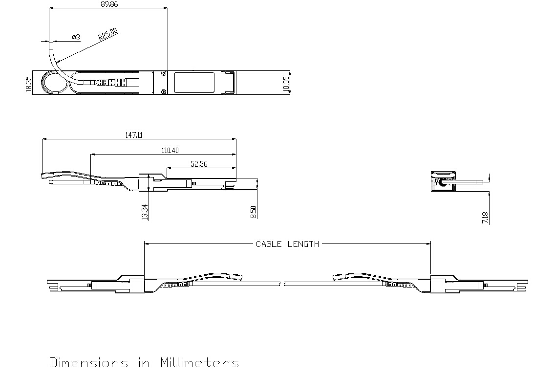
Mechanical Dimensions

ESD
This transceiver is specified as ESD threshold 1KV for high speed data pins and 2KV for all others electrical input pins, tested per MIL-STD-883, Method 3015.4 /JESD22-A114-A (HBM). However, normal ESD precautions are still required during the handling of this module. This transceiver is shipped in ESD protective packaging. It should be removed from the packaging and handled only in an ESD protected environment.
Order Information
|
Part Number |
Product Description |
|
PHQAOC768XX |
40Gb/s QSFP+ Active Optical Cable |
Notes:
where "xx" denotes cable length in meters. Examples are as follows:
xx = 03 for 3m, xx = 10 for 10m, xx = 50 for 50m, xx = A0 for 100m