


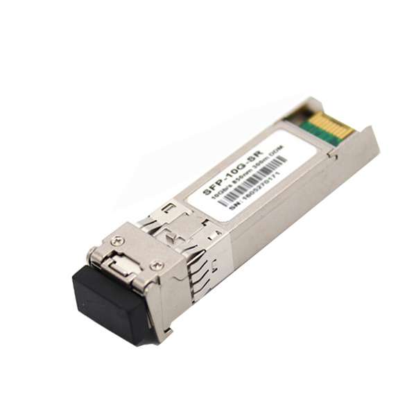

Dongguan Phynam Comtech Co.,Limited
10Gb/s 850nm Multi-mode SFP+ Transceiver
PRODUCT FEATURES
specifications for 10 Gigabit “SFP+”
specifications compliant with SFF 8472
APPLICATIONS
10GBASE-SR/SW 10G Ethernet
STANDARD
PRODUCT SELECTION
DSPM85192LMS
Absolute Maximum Ratings
|
Parameter |
Symbol |
Min |
Typ |
Max |
Unit |
Ref. |
|
Maximum Supply Voltage |
Vcc |
-0.5 |
|
4.7 |
V |
|
|
Storage Temperature |
TS |
-40 |
|
85 |
°C |
|
|
Case Operating Temperature |
Tcase |
-5 |
|
70 |
°C |
|
Electrical Characteristics (Tcase = -5 to 70℃, VCC = 3.14 to 3.46Volts)
|
Parameter |
Symbol |
Min |
Typ |
Max |
Unit |
Ref. |
|
Supply Voltage |
Vcc |
3.14 |
3.3 |
3.46 |
V |
|
|
Supply Current |
Icc |
|
|
250 |
mA |
|
|
Transmitter |
|
|
|
|
|
|
|
Input differential impedance |
Rin |
|
100 |
|
Ω |
1 |
|
Single ended data input swing |
Vin,pp |
180 |
|
700 |
mV |
|
|
Transmit Disable Voltage |
VD |
Vcc–1.3 |
|
Vcc |
V |
|
|
Transmit Enable Voltage |
VEN |
Vee |
|
Vee+ 0.8 |
V |
2 |
|
Transmit Disable Assert Time |
|
|
|
10 |
us |
|
|
Receiver |
|
|
|
|
|
|
|
Differential data output swing |
Vout,pp |
300 |
|
850 |
mV |
3 |
|
Data output rise time |
tr |
|
38 |
ps |
4 |
|
|
Data output fall time |
tf |
|
38 |
ps |
4 |
|
|
LOS Fault |
VLOS fault |
Vcc–1.3 |
|
VccHOST |
V |
5 |
|
LOS Normal |
VLOS norm |
Vee |
|
Vee+0.8 |
V |
5 |
|
Power Supply Rejection |
PSR |
100 |
|
|
mVpp |
6 |
Notes:
Optical Characteristics (Tcase = -5 to70℃, VCC = 3.14 to 3.46 Volts)
|
Parameter |
Symbol |
Min |
Typ |
Max |
Unit |
Ref. |
|
Transmitter |
|
|
|
|
|
|
|
Output Opt. Pwr |
POUT |
-6 |
-1 |
dBm |
1 |
|
|
Optical Wavelength |
λ |
840 |
850 |
860 |
nm |
|
|
Wavelength Temperature Dependance |
0.08 |
0.125 |
nm/°C |
|||
|
Spectral Width (RMS) |
σ |
0.45 |
nm |
|||
|
Optical Extinction Ratio |
ER |
3.0 |
dB |
|||
|
Transmitter and Dispersion Peanlty |
TDP |
3.9 |
dB |
|||
|
RIN |
RIN |
-128 |
dB/Hz |
|||
|
Transmitter Jitter (peak to peak) |
IEEE 802.3.ae requirements |
|||||
|
Receiver |
||||||
|
Average Rx Sensitivity @ 10.325G |
RSENS3 |
-10 |
dBm |
2 |
||
|
Maximum Input Power |
PMAX |
0.5 |
dBm |
|||
|
Optical Center Wavelength |
λC |
840 |
850 |
860 |
nm |
|
|
LOS De -Assert |
LOSD |
-14 |
dBm |
|||
|
LOS Assert |
LOSA |
-30 |
dBm |
|||
|
LOS Hysteresis |
0.5 |
dB |
||||
Notes:
Pin Assignment
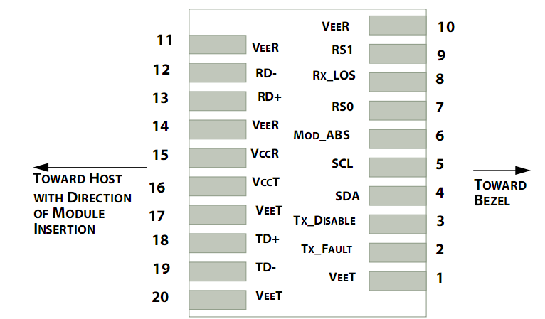
Pin out of Connector Block on Host Board
Pin Descriptions
|
Pin |
Symbol |
Name/Description |
Ref. |
|
1 |
VEET |
Transmitter Ground (Common with Receiver Ground) |
1 |
|
2 |
TFAULT |
Transmitter Fault. |
2 |
|
3 |
TDIS |
Transmitter Disable. Laser output disabled on high or open. |
3 |
|
4 |
SDA |
2-wire Serial Interface Data Line |
4 |
|
5 |
SCL |
2-wire Serial Interface Clock Line |
4 |
|
6 |
MOD_ABS |
Module Absent. Grounded within the module |
4 |
|
7 |
RS0 |
RS0 for Rate Select: Open or Low = Module supports 1.25 Gb/s High = Module supports 9.95 Gb/s to 10.3125 Gb/s |
5 |
|
8 |
LOS |
Loss of Signal indication. Logic 0 indicates normal operation. |
6 |
|
9 |
RS1 |
No connection required |
1 |
|
10 |
VEER |
Receiver Ground (Common with Transmitter Ground) |
1 |
|
11 |
VEER |
Receiver Ground (Common with Transmitter Ground) |
1 |
|
12 |
RD- |
Receiver Inverted DATA out. AC Coupled |
|
|
13 |
RD+ |
Receiver Non-inverted DATA out. AC Coupled |
|
|
14 |
VEER |
Receiver Ground (Common with Transmitter Ground) |
1 |
|
15 |
VCCR |
Receiver Power Supply |
|
|
16 |
VCCT |
Transmitter Power Supply |
|
|
17 |
VEET |
Transmitter Ground (Common with Receiver Ground) |
1 |
|
18 |
TD+ |
Transmitter Non-Inverted DATA in. AC Coupled. |
|
|
19 |
TD- |
Transmitter Inverted DATA in. AC Coupled. |
|
|
20 |
VEET |
Transmitter Ground (Common with Receiver Ground) |
1 |
Notes:
Digital Diagnostic Functions
The SFP+ transceivers support the 2-wire serial communication protocol as defined in the SFP MSA1.
The standard SFP serial ID provides access to identification information that describes the transceiver’s capabilities, standard interfaces, manufacturer, and other information.
Additionally, SFP+ transceivers provide a unique enhanced digital diagnostic monitoring interface, which allows real-time access to device operating parameters such as transceiver temperature, laser bias current, transmitted optical power, received optical power and transceiver supply voltage. It also defines a sophisticated system of alarm and warning flags, which alerts end-users when particular operating parameters are outside of a factory set normal range.
The SFP MSA defines a 256-byte memory map in EEPROM that is accessible over a 2-wire serial interface at the 8 bit address 1010000X (A0h). The digital diagnostic monitoring interface makes use of the 8 bit address 1010001X (A2h), so the originally defined serial ID memory map remains unchanged.
The operating and diagnostics information is monitored and reported by a Digital Diagnostics Transceiver Controller (DDTC) inside the transceiver, which is accessed through a 2-wire serial interface. When the serial protocol is activated, the serial clock signal (SCL, Mod Def 1) is generated by the host. The positive edge clocks data into the SFP transceiver into those segments of the E2PROM that are not write-protected. The negative edge clocks data from the SFP transceiver. The serial data signal (SDA, Mod Def 2) is bi-directional for serial data transfer. The host uses SDA in conjunction with SCL to mark the start and end of serial protocol activation. The memories are organized as a series of 8-bit data words that can be addressed individually or sequentially.
Digital diagnostics for the YAM-85192-5LS are internally calibrated by default.
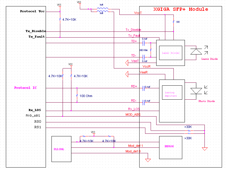
Host - Transceiver Interface Block Diagram
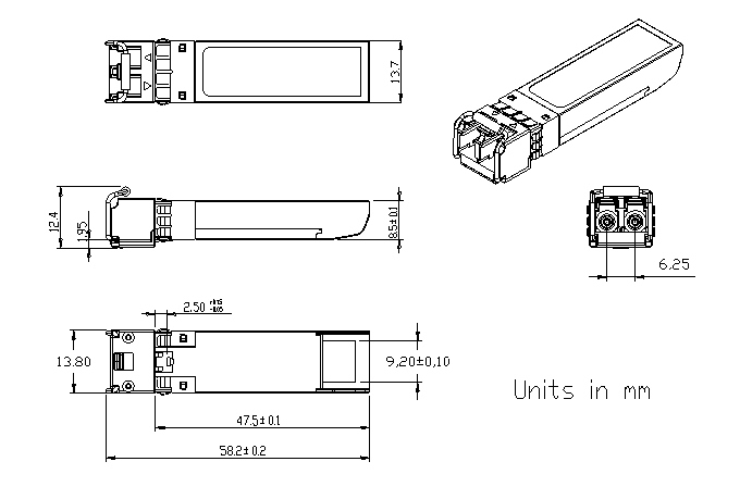
Outline Dimensions
Comply to SFF-8432 rev5.0, the improved Pluggable form factor specification.
Regulatory Compliance
|
Feature |
Reference |
Performance |
|
Electrostatic Discharge (ESD) to the Electrical pin(HBM) |
MIL-STD-883E Method 3015.7 EIA-JESD22-A114 |
Class 1 |
|
(ESD) to the Simplex Receptacle |
IEC/EN 61000-4-2 |
Compatible with standards |
|
Electromagnetic Interference (EMI) |
FCC Part 15 Class B EN 55022 Class B (CISPR 22A) |
Compatible with standards |
|
Laser Eye Safety |
FDA 21CFR 1040.10, 1040.11 IEC/EN 60825-1,2 |
Class 1 laser product |
|
Component Recognition |
IEC/EN 60950 ,UL |
Compatible with standards |
|
ROHS |
2002/95/EC |
Compatible with standards |
