


Dongguan Phynam Comtech Co.,Limited
1.25Gb/s SFP BIDI 20km Optical Transceiver Module
Features
Commercial: 0 ~ +70oC
Extended: -10 ~ +80oC
Industrial: -40 ~ +85oC
Applications
1. Absolute Maximum Ratings
It has to be noted that the operation in excess of any individual absolute maximum ratings might cause permanent damage to this module.
|
Parameter |
Symbol |
Min |
Max |
Unit |
Notes |
|
Storage Temperature |
TS |
-40 |
85 |
oC |
|
|
Power Supply Voltage |
VCC |
-0.3 |
3.6 |
V |
|
|
Relative Humidity (non-condensation) |
RH |
5 |
95 |
% |
|
|
Damage Threshold |
THd |
5 |
dBm |
2. Recommended Operating Conditions and Power Supply Requirements
|
Parameter |
Symbol |
Min |
Typical |
Max |
Unit |
Notes |
|
Operating Case Temperature |
TOP |
0 |
70 |
oC |
commercial |
|
|
-10 |
80 |
extended |
||||
|
-40 |
85 |
industrial |
||||
|
Power Supply Voltage |
VCC |
3.135 |
3.3 |
3.465 |
V |
|
|
Data Rate |
1.25 |
Gb/s |
||||
|
Control Input Voltage High |
2 |
Vcc |
V |
|||
|
Control Input Voltage Low |
0 |
0.8 |
V |
|||
|
Link Distance (SMF) |
D |
20 |
km |
9/125um |
3. General Description
The Small Form Factor Pluggable (SFP) transceivers are compatible with the Small Form Factor Pluggable Multi-Sourcing Agreement (MSA), The transceiver consists of five sections: the LD driver, the limiting amplifier, the digital diagnostic monitor, the DFB laser and the PIN photo-detector .The module data link up to 20km in 9/125um single mode fiber.
The optical output can be disabled by a TTL logic high-level input of Tx Disable, and the system also can disable the module via I2C. Tx Fault is provided to indicate that degradation of the laser. Loss of signal (LOS) output is provided to indicate the loss of an input optical signal of receiver or the link status with partner. The system can also get the LOS (or Link)/Disable/Fault information via I2C register access.
4. Pin Assignment and Pin Description
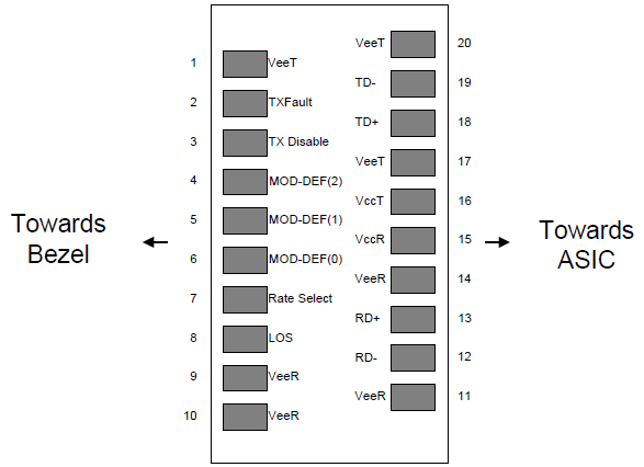
Figure1. Diagram of host board connector block pin numbers and names
|
PIN |
Name |
Name/Description |
Notes |
|
1 |
VEET |
Transmitter Ground (Common with Receiver Ground) |
1 |
|
2 |
TXFAULT |
Transmitter Fault. |
|
|
3 |
TXDIS |
Transmitter Disable. Laser output disabled on high or open. |
2 |
|
4 |
MOD_DEF(2) |
Module Definition 2. Data line for Serial ID. |
3 |
|
5 |
MOD_DEF(1) |
Module Definition 1. Clock line for Serial ID. |
3 |
|
6 |
MOD_DEF(0) |
Module Definition 0. Grounded within the module. |
3 |
|
7 |
Rate Select |
No connection required |
4 |
|
8 |
LOS |
Loss of Signal indication. Logic 0 indicates normal operation. |
5 |
|
9 |
VEER |
Receiver Ground (Common with Transmitter Ground) |
1 |
|
10 |
VEER |
Receiver Ground (Common with Transmitter Ground) |
1 |
|
11 |
VEER |
Receiver Ground (Common with Transmitter Ground) |
1 |
|
12 |
RD- |
Receiver Inverted DATA out. AC Coupled |
|
|
13 |
RD+ |
Receiver Non-inverted DATA out. AC Coupled |
|
|
14 |
VEER |
Receiver Ground (Common with Transmitter Ground) |
1 |
|
15 |
VCCR |
Receiver Power Supply |
|
|
16 |
VCCT |
Transmitter Power Supply |
|
|
17 |
VEET |
Transmitter Ground (Common with Receiver Ground) |
1 |
|
18 |
TD+ |
Transmitter Non-Inverted DATA in. AC Coupled. |
|
|
19 |
TD- |
Transmitter Inverted DATA in. AC Coupled. |
|
|
20 |
VEET |
Transmitter Ground (Common with Receiver Ground) |
1 |
Notes:
1. Circuit ground is internally isolated from chassis ground.
2. Laser output disabled on TDIS >2.0V or open, enabled on TDIS <0.8V.
3. Should be pulled up with 4.7k - 10kohms on host board to a voltage between 2.0V and 3.6V.MOD_DEF (0) pulls line low to indicate module is plugged in.
4. This is an optional input used to control the receiver bandwidth for compatibility with multiple data rates (most likely Fiber Channel 1x and 2x Rates).If implemented, the input will be internally pulled down with > 30kΩ resistor. The input states are:
1) Low (0 – 0.8V): Reduced Bandwidth
2) (>0.8, < 2.0V): Undefined
3) High (2.0 – 3.465V): Full Bandwidth
4) Open: Reduced Bandwidth
5. LOS is open collector output should be pulled up with 4.7k - 10kohms on host board to a voltage between 2.0V and 3.6V. Logic 0 indicates normal operation; logic 1 indicates loss of signal.
5. Electrical Characteristics
The following electrical characteristics are defined over the Recommended Operating Environment unless otherwise specified.
|
Parameter |
Symbol |
Min. |
Typical |
Max |
Unit |
Notes |
|
|
Power Consumption |
P |
0.86 |
W |
commercial |
|||
|
0.95 |
Industrial |
||||||
|
Supply Current |
Icc |
260 |
mA |
commercial |
|||
|
280 |
Industrial |
||||||
|
Transmitter |
|||||||
|
Single-ended Input Voltage Tolerance |
VCC |
-0.3 |
4.0 |
V |
|||
|
Differential Input Voltage Swing |
Vin,pp |
200 |
2400 |
mVpp |
|||
|
Differential Input Impedance |
Zin |
90 |
100 |
110 |
Ohm |
||
|
Transmit Disable Assert Time |
5 |
us |
|||||
|
Transmit Disable Voltage |
Vdis |
Vcc-1.3 |
Vcc |
V |
|||
|
Transmit Enable Voltage |
Ven |
Vee-0.3 |
0.8 |
V |
|||
|
Receiver |
|||||||
|
Differential Output Voltage Swing |
Vout,pp |
500 |
900 |
mVpp |
|||
|
Differential Output Impedance |
Zout |
90 |
100 |
110 |
Ohm |
||
|
Data output rise/fall time |
Tr/Tf |
100 |
ps |
20% to 80% |
|||
|
LOS Assert Voltage |
VlosH |
Vcc-1.3 |
Vcc |
V |
|||
|
LOS De-assert Voltage |
VlosL |
Vee-0.3 |
0.8 |
V |
|||
6. Optical Characteristics
|
Parameter |
Symbol |
Min. |
Typical |
Max |
Unit |
Notes |
|
|
Transmitter |
|||||||
|
Center Wavelength |
λC |
1530 |
1550 |
1570 |
nm |
||
|
Spectrum Bandwidth(RMS) |
σ |
1 |
nm |
||||
|
Side Mode Suppression Ratio |
SMSR |
30 |
dB |
||||
|
Average Optical Power |
PAVG |
-9 |
-3 |
dBm |
1 |
||
|
Optical Extinction Ratio |
ER |
9 |
dB |
||||
|
Transmitter OFF Output Power |
POff |
-45 |
dBm |
||||
|
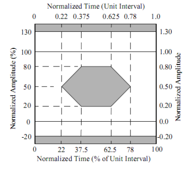
Transmitter Eye Mask |
Compliant with 802.3z(class 1 laser safety) |
2 |
|||||
|
Receiver |
|||||||
|
Center Wavelength |
λC |
1290 |
1310 |
1330 |
nm |
||
|
Receiver Sensitivity (Average Power) |
Sen. |
-20 |
dBm |
3 |
|||
|
Input Saturation Power (overload) |
Psat |
-3 |
dBm |
||||
|
LOS Assert |
LOSA |
-36 |
dB |
4 |
|||
|
LOS De-assert |
LOSD |
-21 |
dBm |
4 |
|||
|
LOS Hysteresis |
LOSH |
0.5 |
2 |
6 |
dBm |
||
The following optical characteristics are defined over the Recommended Operating Environment unless otherwise specified.
 Notes:
1. Measure at 2^7-1 NRZ PRBS pattern
2. Transmitter eye mask definition.
3. Measured with Light source 1550nm, ER=9dB; BER =<10^-12 @PRBS=2^7-1 NRZ
4. When LOS de-asserted, the RX data+/- output is High-level (fixed).
7. Digital Diagnostic Functions
|
Parameter |
Symbol |
Min. |
Max |
Unit |
Notes |
|
Temperature monitor absolute error |
DMI_ Temp |
-3 |
3 |
degC |
Over operating temp |
|
Supply voltage monitor absolute error |
DMI _VCC |
-0.15 |
0.15 |
V |
Full operating range |
|
RX power monitor absolute error |
DMI_RX |
-3 |
3 |
dB |
|
|
Bias current monitor |
DMI_ bias |
-10% |
10% |
mA |
|
|
TX power monitor absolute error |
DMI_TX |
-3 |
3 |
dB |
The following digital diagnostic characteristics are defined over the Recommended Operating Environment unless otherwise specified. It is compliant to SFF8472 Rev10.2 with internal calibration mode. For external calibration mode please contact our sales staff.
|
Parameter |
Symbol |
Min. |
Max |
Unit |
Notes |
|
Temperature monitor absolute error |
DMI_ Temp |
-3 |
3 |
degC |
Over operating temp |
|
Supply voltage monitor absolute error |
DMI _VCC |
-0.15 |
0.15 |
V |
Full operating range |
|
RX power monitor absolute error |
DMI_RX |
-3 |
3 |
dB |
|
|
Bias current monitor |
DMI_ bias |
-10% |
10% |
mA |
|
|
TX power monitor absolute error |
DMI_TX |
-3 |
3 |
dB |
8. Mechanical Dimensions
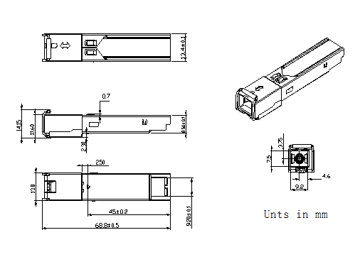
Figure2. Mechanical Outline
