


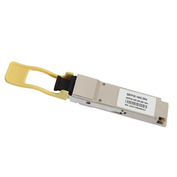


Dongguan Phynam Comtech Co.,Limited
100Gb/s QSFP28 SR4 Optical Transceiver Module
PH-QSFP28/100G-SR4
Features
Applications
1.General Description
This product is a parallel 100Gb/s Quad Small Form-factor Pluggable (QSFP28) optical module. It provides increased port density and total system cost savings. The QSFP28 full-duplex optical module offers 4 independent transmit and receive channels, each capable of 25Gb/s operation for an aggregate data rate of 100Gb/s on 100 meters of OM4 multi-mode fiber.
An optical fiber ribbon cable with an MTP/MPO connector can be plugged into the QSFP28 module receptacle. Proper alignment is ensured by the guide pins inside the receptacle. The cable usually cannot be twisted for proper channel to channel alignment. Electrical connection is achieved through an MSA-compliant 38-pin edge type connector.
The module operates by a single +3.3V power supply. LVCMOS/LVTTL global control signals, such as Module Present, Reset, Interrupt and Low Power Mode, are available with the modules. A 2-wire serial interface is available to send and receive more complex control signals, and to receive digital diagnostic information. Individual channels can be addressed and unused channels can be shut down for maximum design flexibility.
The product is designed with form factor, optical/electrical connection and digital diagnostic interface according to the QSFP28 Multi-Source Agreement (MSA). It has been designed to meet the harshest external operating conditions including temperature, humidity and EMI interference. The module offers very high functionality and feature integration, accessible via a two-wire serial interface.
2.Functional Description
This product converts parallel electrical input signals into parallel optical signals, by a driven Vertical Cavity Surface Emitting Laser (VCSEL) array. The transmitter module accepts electrical input signals compatible with Common Mode Logic (CML) levels. All input data signals are differential and internally terminated. The receiver module converts parallel optical input signals via a photo detector array into parallel electrical output signals. The receiver module outputs electrical signals are also voltage compatible with Common Mode Logic (CML) levels. All data signals are differential and support a data rates up to 25Gb/s per channel. Figure 1 shows the functional block diagram of this product.
A single +3.3V power supply is required to power up the module. Both power supply pins VccTx and VccRx are internally connected and should be applied concurrently. As per MSA specifications the module offers 7 low speed hardware control pins (including the 2-wire serial interface): ModSelL, SCL, SDA, ResetL, LPMode, ModPrsL and IntL.
Module Select (ModSelL) is an input pin. When held low by the host, the module responds to 2-wire serial communication commands. The ModSelL allows the use of multiple QSFP28 modules on a single 2-wire interface bus – individual ModSelL lines for each QSFP28 module must be used.
Serial Clock (SCL) and Serial Data (SDA) are required for the 2-wire serial bus communication interface and enable the host to access the QSFP28 memory map.
The ResetL pin enables a complete module reset, returning module settings to their default state, when a low level on the ResetL pin is held for longer than the minimum pulse length. During the execution of a reset the host shall disregard all status bits until the module indicates a completion of the reset interrupt. The module indicates this by posting an IntL (Interrupt) signal with the Data_Not_Ready bit negated in the memory map. Note that on power up (including hot insertion) the module should post this completion of reset interrupt without requiring a reset.
Low Power Mode (LPMode) pin is used to set the maximum power consumption for the module in order to protect hosts that are not capable of cooling higher power modules, should such modules be accidentally inserted.
Module Present (ModPrsL) is a signal local to the host board which, in the absence of a module, is normally pulled up to the host Vcc. When a module is inserted into the connector, it completes the path to ground through a resistor on the host board and asserts the signal. ModPrsL then indicates a module is present by setting ModPrsL to a “Low” state.
Interrupt (IntL) is an output pin. Low indicates a possible module operational fault or a status critical to the host system. The host identifies the source of the interrupt using the 2-wire serial interface. The IntL pin is an open collector output and must be pulled to the Host Vcc voltage on the Host board.
3.Transceiver Block Diagram
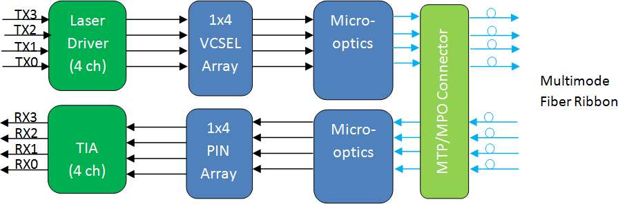 Figure 1. Transceiver Block Diagram
4.Pin Assignment and Description
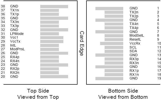
Figure 2. MSA Compliant Connector
|
PIN |
Logic |
Symbol |
Name/Description |
Notes |
|
1 |
GND |
Ground |
1 |
|
|
2 |
CML-I |
Tx2n |
Transmitter Inverted Data Input |
|
|
3 |
CML-I |
Tx2p |
Transmitter Non-Inverted Data output |
|
|
4 |
GND |
Ground |
1 |
|
|
5 |
CML-I |
Tx4n |
Transmitter Inverted Data Input |
|
|
6 |
CML-I |
Tx4p |
Transmitter Non-Inverted Data output |
|
|
7 |
GND |
Ground |
1 |
|
|
8 |
LVTLL-I |
ModSelL |
Module Select |
|
|
9 |
LVTLL-I |
ResetL |
Module Reset |
|
|
10 |
VccRx |
+3.3V Power Supply Receiver |
2 |
|
|
11 |
LVCMOS-I/O |
SCL |
2-Wire Serial Interface Clock |
|
|
12 |
LVCMOS-I/O |
SDA |
2-Wire Serial Interface Data |
|
|
13 |
GND |
Ground |
||
|
14 |
CML-O |
Rx3p |
Receiver Non-Inverted Data Output |
|
|
15 |
CML-O |
Rx3n |
Receiver Inverted Data Output |
|
|
16 |
GND |
Ground |
1 |
|
|
17 |
CML-O |
Rx1p |
Receiver Non-Inverted Data Output |
|
|
18 |
CML-O |
Rx1n |
Receiver Inverted Data Output |
|
|
19 |
GND |
Ground |
1 |
|
|
20 |
GND |
Ground |
1 |
|
|
21 |
CML-O |
Rx2n |
Receiver Inverted Data Output |
|
|
22 |
CML-O |
Rx2p |
Receiver Non-Inverted Data Output |
|
|
23 |
GND |
Ground |
1 |
|
|
24 |
CML-O |
Rx4n |
Receiver Inverted Data Output |
1 |
|
25 |
CML-O |
Rx4p |
Receiver Non-Inverted Data Output |
|
|
26 |
GND |
Ground |
1 |
|
|
27 |
LVTTL-O |
ModPrsL |
Module Present |
|
|
28 |
LVTTL-O |
IntL |
Interrupt |
|
|
29 |
VccTx |
+3.3 V Power Supply transmitter |
2 |
|
|
30 |
Vcc1 |
+3.3 V Power Supply |
2 |
|
|
31 |
LVTTL-I |
LPMode |
Low Power Mode |
|
|
32 |
GND |
Ground |
1 |
|
|
33 |
CML-I |
Tx3p |
Transmitter Non-Inverted Data Input |
|
|
34 |
CML-I |
Tx3n |
Transmitter Inverted Data Output |
|
|
35 |
GND |
Ground |
1 |
|
|
36 |
CML-I |
Tx1p |
Transmitter Non-Inverted Data Input |
|
|
37 |
CML-I |
Tx1n |
Transmitter Inverted Data Output |
|
|
38 |
GND |
Ground |
1 |
Notes:
1. GND is the symbol for signal and supply (power) common for QSFP28 modules. All are
common within the QSFP28 module and all module voltages are referenced to this potential
unless otherwise noted. Connect these directly to the host board signal common ground plane.
2. VccRx, Vcc1 and VccTx are the receiver and transmitter power suppliers and shall be applied
concurrently. Recommended host board power supply filtering is shown in Figure 4 below. Vcc
Rx, Vcc1 and Vcc Tx may be internally connected within the QSFP28 transceiver module in any
combination. The connector pins are each rated for a maximum current of 1000mA.
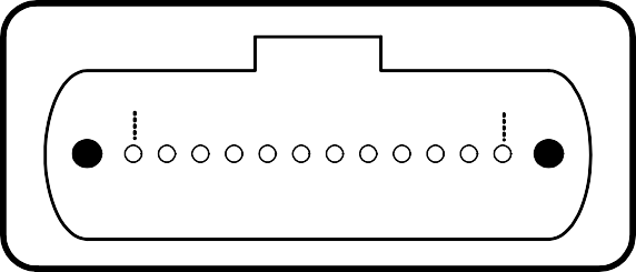
5.Optical Interface Lanes and Assignment
Figure 3 shows the orientation of the multi-mode fiber facets of the optical connector. Table 1 provides the lane assignment.
Fiber 12
Fiber 1
Figure 3. Outside View of the QSFP28 Module MPO Receptacle
Table 1: Lane Assignment
|
Fiber # |
Lane Assignment |
|
1 |
RX0 |
|
2 |
RX1 |
|
3 |
RX2 |
|
4 |
RX3 |
|
5,6,7,8 |
Not used |
|
9 |
TX3 |
|
10 |
TX2 |
|
11 |
TX1 |
|
12 |
TX0 |
6.Recommended Power Supply Filter
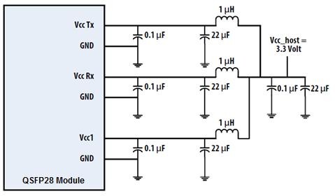
Figure 4. Recommended Power Supply Filter
7.Absolute Maximum Ratings
It has to be noted that the operation in excess of any individual absolute maximum ratings might cause permanent damage to this module.
|
Parameter |
Symbol |
Min |
Max |
Units |
Note |
|
Storage Temperature |
TS |
-40 |
85 |
degC |
|
|
Operating Case Temperature |
TOP |
0 |
70 |
degC |
|
|
Power Supply Voltage |
VCC |
-0.5 |
3.6 |
V |
|
|
Relative Humidity (non-condensation) |
RH |
0 |
85 |
% |
|
|
Damage Threshold, each Lane |
THd |
3.4 |
dBm |
8.Recommended Operating Conditions and Power Supply Requirements
|
Parameter |
Symbol |
Min |
Typical |
Max |
Units |
Notes |
|
Operating Case Temperature |
TOP |
0 |
70 |
degC |
||
|
Power Supply Voltage |
VCC |
3.135 |
3.3 |
3.465 |
V |
|
|
Data Rate, each Lane |
25.78125 |
Gb/s |
||||
|
Data Rate Accuracy |
-100 |
100 |
ppm |
|||
|
Pre-FEC Bit Error Ratio |
5x10⁻⁵ |
|||||
|
Post-FEC Bit Error Ratio |
1x10-12 |
1 |
||||
|
Control Input Voltage High |
2 |
Vcc |
V |
|||
|
Control Input Voltage Low |
0 |
0.8 |
V |
|||
|
Link Distance (OM3 MMF) |
D1 |
70 |
m |
2 |
||
|
Link Distance (OM4 MMF) |
D2 |
100 |
m |
2 |
Notes:
1.FEC provided by host system.
2.FEC required on host system to support maximum distance.
9.Electrical Characteristics
The following electrical characteristics are defined over the Recommended Operating Environment unless otherwise specified.
|
Parameter |
Test Point |
Min |
Typical |
Max |
Units |
Notes |
|
Power Consumption |
2.5 |
W |
||||
|
Supply Current |
Icc |
757 |
mA |
|||
|
Transmitter (each Lane) |
||||||
|
Overload Differential Voltage pk-pk |
TP1a |
900 |
mV |
|||
|
Common Mode Voltage (Vcm) |
TP1 |
-350 |
2850 |
mV |
1 |
|
|
Differential Termination Resistance Mismatch |
TP1 |
10 |
% |
At 1MHz |
||
|
Differential Return Loss (SDD11) |
TP1 |
See CEI- 28G-VSR Equation 13-19 |
dB |
|||
|
Common Mode to Differential conversion and Differential to Common Mode conversion(SDC11, SCD11) |
TP1 |
See CEI- 28G-VSR Equation 13-20 |
dB |
|||
|
Stressed Input Test |
TP1a |
See CEI- 28G-VSR Section 13.3.11.2.1 |
||||
|
Receiver (each Lane) |
||||||
|
Differential Voltage, pk-pk |
TP4 |
900 |
mV |
|||
|
Common Mode Voltage (Vcm) |
TP4 |
-350 |
2850 |
mV |
1 |
|
|
Common Mode Noise, RMS |
TP4 |
17.5 |
mV |
|||
|
Differential Termination Resistance Mismatch |
TP4 |
10 |
% |
At 1MHz |
||
|
Differential Return Loss (SDD22) |
TP4 |
See CEI- 28G-VSR Equation 13-19 |
dB |
|||
|
Common Mode to Differential conversion and Differential to Common Mode conversion(SDC22, SCD22) |
TP4 |
See CEI- 28G-VSR Equation 13-21 |
dB |
|||
|
Common Mode Return Loss (SCC22) |
TP4 |
-2 |
dB |
2 |
||
|
Transition Time, 20 to 80% |
TP4 |
9.5 |
ps |
|||
|
Vertical Eye Closure (VEC) |
TP4 |
5.5 |
dB |
|||
|
Eye Width at 10-15 probability (EW15) |
TP4 |
0.57 |
UI |
|||
|
Eye Height at 10-15 probability (EH15) |
TP4 |
228 |
mV |
|||
Notes:
1.Vcm is generated by the host. Specification includes effects of ground offset voltage.
2.From 250MHz to 30GHz.
10.Optical Characteristics
|
Parameter |
Symbol |
Min |
Typical |
Max |
Units |
Notes |
|
Transmitter |
||||||
|
Center Wavelength |
λC |
840 |
850 |
860 |
nm |
|
|
RMS Spectral Width |
∆λrms |
0.6 |
nm |
|||
|
Average Launch Power, each Lane |
PAVG |
-8.4 |
2.4 |
dBm |
||
|
Optical Modulation Amplitude (OMA), each Lane |
POMA |
-6.4 |
3 |
dBm |
1 |
|
|
Launch Power in OMA minus TDEC, each Lane |
-7.3 |
dBm |
||||
|
Transmitter and Dispersion Eye Closure (TDEC), each Lane |
4.3 |
dB |
||||
|
Extinction Ratio |
ER |
2 |
dB |
|||
|
Optical Return Loss Tolerance |
TOL |
12 |
dB |
|||
|
Average Launch Power OFF Transmitter, each Lane |
Poff |
-30 |
dBm |
|||
|
Encircled Flux |
≥ 86% at 19 μm ≤ 30% at 4.5 μm |
|||||
|
Transmitter Eye Mask Definition {X1, X2, X3, Y1, Y2, Y3} |
{0.3, 0.38, 0.45, 0.35, 0.41, 0.5} |
2 |
||||
|
Receiver |
||||||
|
Center Wavelength |
λC |
840 |
850 |
860 |
nm |
|
|
Damage Threshold, each Lane |
THd |
3.4 |
dBm |
3 |
||
|
Average Receive Power, each Lane |
-10.3 |
2.4 |
dBm |
|||
|
Receive Power (OMA), each Lane Lane |
3 |
dBm |
||||
|
Receiver Sensitivity (OMA), each |
SEN |
-9.2 |
dBm |
for BER = 5x10⁻⁵ |
||
|
Stressed Receiver Sensitivity (OMA), each Lane |
-5.2 |
dBm |
4 |
|||
|
Receiver Reflectance |
RR |
-12 |
dB |
|||
|
LOS Assert |
LOSA |
-30 |
dBm |
|||
|
LOS Deassert |
LOSD |
-12 |
dBm |
|||
|
LOS Hysteresis |
LOSH |
0.5 |
dB |
|||
|
Conditions of Stress Receiver Sensitivity Test (Note 5) |
||||||
|
Stressed Eye Closure (SEC), Lane under Test |
4.3 |
dB |
||||
|
Stressed Eye J2 Jitter, Lane under Test |
0.39 |
UI |
||||
|
Stressed Eye J4 Jitter, Lane under Test |
0.53 |
UI |
||||
|
OMA of each Aggressor Lane |
3 |
dBm |
||||
|
Stressed Receiver Eye Mask Definition {X1, X2, X3, Y1, Y2, Y3},Hit ratio 5x10⁻⁵ hits per sample |
{0.28, 0.5, 0.5, 0.33, 0.33, 0.4} |
|||||
Notes:
1.Even if the TDP < 0.9 dB, the OMA min must exceed the minimum value specified here.
2.Hit ratio 1.5x10⁻³ hits per sample.
3.The receiver shall be able to tolerate, without damage, continuous exposure to a modulated optical input signal having this power level on one lane. The receiver does not have to operate correctly at this input power.
4.Measured with conformance test signal at receiver input for BER = 5x10⁻⁵.
5.Vertical eye closure penalty, stressed eye J2 jitter, stressed eye J4 jitter, and stressed receiver eye mask definition are test conditions for measuring stressed receiver sensitivity. They are not characteristics of the receiver.
11.Digital Diagnostic Functions
The following digital diagnostic characteristics are defined over the Recommended Operating Environment unless otherwise specified. It is compliant to SFF-8436.
|
Parameter |
Symbol |
Min |
Max |
Units |
Notes |
|
Temperature monitor absolute error |
DMI_Temp |
-3 |
3 |
degC |
Over operating temperature range |
|
Supply voltage monitor absolute error |
DMI _VCC |
-0.15 |
0.15 |
V |
Over full operating range |
|
Channel RX power monitor absolute error |
DMI_RX_Ch |
-2 |
2 |
dB |
1 |
|
Channel Bias current monitor |
DMI_Ibias_Ch |
-10% |
10% |
mA |
Ch1~Ch4 |
|
Channel TX power monitor absolute error |
DMI_TX_Ch |
-2 |
2 |
dB |
1 |
Notes:
1.Due to measurement accuracy of different single mode fibers, there could be an additional +/-1 dB fluctuation, or a +/- 3 dB total accuracy.
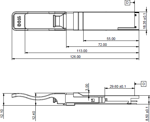
Figure 5. Mechanical Outline
13.ESD
This transceiver is specified as ESD threshold 1kV for high speed data pins and 2kV for all others electrical input pins, tested per MIL-STD-883, Method 3015.4 /JESD22-A114-A (HBM). However, normal ESD precautions are still required during the handling of this module. This transceiver is shipped in ESD protective packaging. It should be removed from the packaging and handled only in an ESD protected environment.
14.Laser Safety
This is a Class 1 Laser Product according to EN 60825-1:2014. This product complies with 21 CFR 1040.10 and 1040.11 except for deviations pursuant to Laser Notice No. 50, dated (June 24, 2007).
Caution: Use of controls or adjustments or performance of procedures other than those specified herein may result in hazardous radiation exposure.
