
Dongguan Phynam Comtech Co.,Limited
Product Specification
1.25Gbps BIDI 20Km SFP Transceiver
PH-SB3512-20LCD PH-SB5312-20LCD
Product Features
|
PART NUMBER |
WAVE LENGTH TX/RX |
DISTANCE |
LASER |
TEMPERATURE |
|
PH-SB3512-20LCD |
Tx1310/Rx1550nm |
20Km |
FP+PIN |
COM 0~70℃ |
|
PH-SB5312-20LCD |
Tx1550/Rx1310nm |
20Km |
DFB+PIN |
COM 0~70℃ |
1. Product Description
The PH-SB3512-20LCD and PH-SB5312-20LCD series SFPs are small form factor pluggable (SFP) transceivers compatible with multi-sourcing agreement (MSA). It is suitable for single-mode fiber (SMF) communications in 1.25Gbps Ethernet and 1G/2G Fiber Channel.
2. Regulatory Compliance
This transceivers are Class 1 Laser Products comply with FDA regulations. Meet Class 1 eye safety requirements of EN 60825 and the electrical safety requirements of EN 60950.
3. Recommended Operating Conditions
|
Parameter |
Symbol |
Min. |
Typical |
Max. |
Unit |
|
|
PH-SB3512-20LCD |
Operating Case Temperature |
TC |
0 |
70 |
°C |
|
|
PH-SB5312-20LCD |
0 |
70 |
||||
|
Power Supply Voltage |
VCC |
3.15 |
3.3 |
3.45 |
V |
|
|
Power Supply Current |
ICC |
300 |
mA |
|||
|
Data Rate |
1.25 |
GBps |
||||
4. Optical Characteristics
PH-SB3512-20LCD
|
Parameter |
Symbol |
Min. |
Typical |
Max. |
Unit |
|
Transmitter |
|||||
|
Centre Wavelength |
λc |
1270 |
1310 |
1370 |
nm |
|
Spectral Width (RMS) |
σ |
4 |
nm |
||
|
Average Output Power |
Pout |
-9 |
-3 |
dBm |
|
|
Extinction Ratio |
EX |
9 |
dB |
||
|
Optical Rise/Fall Time |
tr/tf |
2 |
ns |
||
|
Receiver |
|||||
|
Centre Wavelength |
λc |
1510 |
1550 |
1590 |
nm |
|
Receiver Sensitivity |
PIN |
-22 |
dBm |
||
|
Receiver Overload |
PMAX |
1 |
|
dBm |
|
|
LOS De-Assert |
LOSD |
-30 |
dBm |
||
|
LOS Assert |
LOSA |
-35 |
dBm |
||
|
LOS Hysteresis |
0.5 |
4.5 |
dB |
||
PH-SB5312-20LCD
|
Parameter |
Symbol |
Min. |
Typical |
Max. |
Unit |
|
Transmitter |
|||||
|
Centre Wavelength |
λc |
1530 |
1550 |
1570 |
nm |
|
Spectral Width (RMS) |
σ |
4 |
nm |
||
|
Average Output Power |
Pout |
-9 |
-3 |
dBm |
|
|
Extinction Ratio |
EX |
9 |
dB |
||
|
Optical Rise/Fall Time |
tr/tf |
2 |
ns |
||
|
Receiver |
|||||
|
λc |
1270 |
1310 |
1350 |
nm |
|
|
Receiver Sensitivity |
PIN |
-22 |
dBm |
||
|
Receiver Overload |
PMAX |
1 |
|
dBm |
|
|
LOS De-Assert |
LOSD |
-30 |
dBm |
||
|
LOS Assert |
LOSA |
-35 |
dBm |
||
|
LOS Hysteresis |
0.5 |
4.5 |
dB |
||
5. Electrical Characteristics
|
Parameter |
Symbol |
Min. |
Typical |
Max. |
Unit |
|
Transmitter |
|||||
|
Input Differential Impedance |
Zin |
90 |
100 |
110 |
Ω |
|
Data Input Swing Differential |
Vin |
500 |
2400 |
mV |
|
|
Tx-Dis Disable |
Vd |
2.0 |
Vcc |
V |
|
|
Tx-Dis Enable |
Ven |
0 |
0.8 |
V |
|
|
TX-Fault (Fault) |
2.0 |
Vcc+0.3 |
V |
||
|
TX-Fault (Normal) |
0 |
0.8 |
V |
||
|
Receiver |
|||||
|
Data Output Swing Differential |
Vout |
370 |
2000 |
mV |
|
|
Rx-Los Fault |
Vlf |
2.0 |
Vcc+0.3 |
V |
|
|
Rx-Los Normal |
Vln |
0 |
0+0.8 |
V |
|
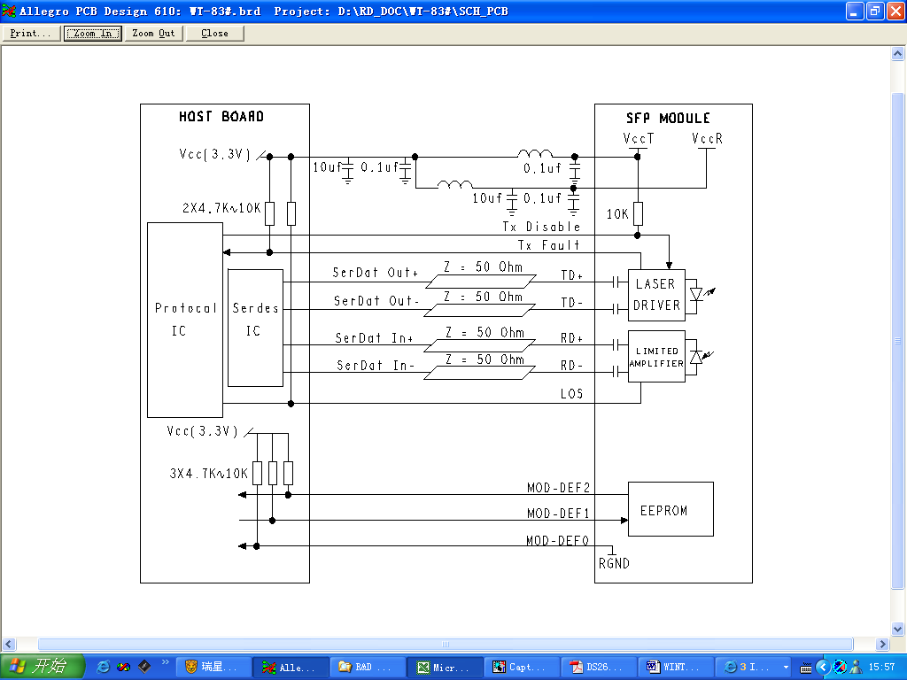
6. Pin Descriptions
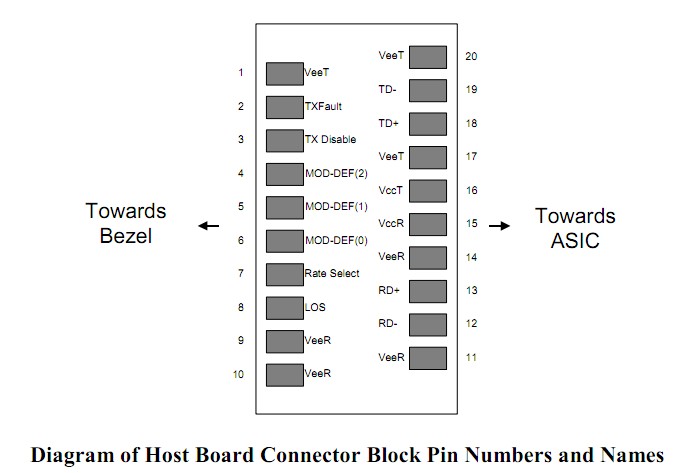
|
Pin |
Symbol |
Description |
Ref. |
|
1 |
VEET |
Transmitter Ground (Common with Receiver Ground) |
6.1 |
|
2 |
TFAULT |
Transmitter Fault. Not supported. |
|
|
3 |
TDIS |
Transmitter Disable. Laser output disabled on high or open. |
6.2 |
|
4 |
MOD_DEF(2) |
Module Definition 2. Data line for Serial ID. |
6.3 |
|
5 |
MOD_DEF(1) |
Module Definition 1. Clock line for Serial ID. |
6.3 |
|
6 |
MOD_DEF(0) |
Module Definition 0. Grounded within the module. |
6.3 |
|
7 |
Rate Select |
No connection required |
|
|
8 |
LOS |
Loss of Signal indication. Logic 0 indicates normal operation. |
6.4 |
|
9 |
VEER |
Receiver Ground (Common with Transmitter Ground) |
6.1 |
|
10 |
VEER |
Receiver Ground (Common with Transmitter Ground) |
6.1 |
|
11 |
VEER |
Receiver Ground (Common with Transmitter Ground) |
6.1 |
|
12 |
RD- |
Receiver Inverted DATA out. AC Coupled. |
|
|
13 |
RD+ |
Receiver Non-inverted DATA out. AC Coupled. |
|
|
14 |
VEER |
Receiver Ground (Common with Transmitter Ground) |
6.1 |
|
15 |
VCCR |
Receiver Power Supply |
|
|
16 |
VCCT |
Transmitter Power Supply |
|
|
17 |
VEET |
Transmitter Ground (Common with Receiver Ground) |
6.1 |
|
18 |
TD+ |
Transmitter Non-Inverted DATA in. AC Coupled. |
|
|
19 |
TD- |
Transmitter Inverted DATA in. AC Coupled. |
|
|
20 |
VEET |
Transmitter Ground (Common with Receiver Ground) |
6.1 |
Notes:
6.1 Circuit ground is internally isolated from chassis ground.
6.2 Laser output disabled on TDIS >2.0V or open, enabled on TDIS <0.8V.
6.3 Should be pulled up with 4.7k - 10kohms on host board to a voltage between 2.0V and 3.6V. MOD_DEF(0) pulls line low to indicate module is plugged in.
6.4 LOS is open collector output. Should be pulled up with 4.7k -10kohms on host board to a voltage between 2.0V and 3.6V. Logic 0 indicates normal operation; logic 1 indicates loss of signal.
8. EEPROM & DDM THRESHOLD
8.1 EEPROM
2 wire address 1010000X (A0hex)
|
0~95 Serial ID Defined by SFP MSA (96 bytes) |
|
96~127 Vendor Speific (32 bytes) |
|
128~255 Reserved (128 bytes) |
EEPROM Serial ID Memory Contents
|
Add. |
Size (Bytes) |
Name of Field |
Hex |
Description |
|
BASE ID FIELDS |
||||
|
0 |
1 |
Identifier |
03 |
SFP |
|
1 |
1 |
Ext. Identifier |
04 |
SFP function is defined by serial ID only |
|
2 |
1 |
Connector |
07 |
LC |
|
3-10 |
8 |
Transceiver |
00 10 02 00 00 00 00 00 |
Transmitter Code |
|
11 |
1 |
Encoding |
01 |
GE |
|
12 |
1 |
BR, Nominal |
0D |
1300M bps |
|
13 |
1 |
Reserved |
00 |
|
|
14 |
1 |
Length (9um) km |
14 |
20Km |
|
15 |
1 |
Length (9um) km |
C8 |
|
|
16 |
1 |
OM2 Length (50um) m |
00 |
|
|
17 |
1 |
OM1 Length (62.5um) m |
00 |
|
|
18 |
1 |
Length (Copper) |
00 |
|
|
19 |
1 |
OM3 Length (50um) m |
00 |
|
|
20-35 |
16 |
Vendor Name |
48 41 4E 44 41 52 20 20 20 20 20 20 20 20 20 20 |
HANDAR * OEM available |
|
36 |
1 |
Reserved |
00 |
|
|
37-39 |
3 |
Vendor OUI |
00 00 00 |
* OEM available |
|
40-55 |
16 |
Vendor PN |
xx xx xx xx xx xx xx xx xx xx xx xx xx xx xx xx |
* OEM available |
|
56-59 |
4 |
Vendor Rev |
30 31 20 20 |
01 |
|
60-61 |
2 |
Wavelength |
05 IE/ 06 0E/05 D2 |
1310nm/ 1550nm/1490nm |
|
62 |
1 |
Reserved |
00 |
|
|
63 |
1 |
CC_BASE |
xx |
Check Code for Base ID Field |
|
EXTENDED ID FIELDS |
||||
|
64-65 |
2 |
Options |
00 1A |
Loss/ TX_Fault/ TX_Disable |
|
66 |
1 |
BR, Max |
00 |
|
|
67 |
1 |
BR, Min |
00 |
|
|
68-83 |
16 |
Vendor SN |
43 4C xx xx xx xx xx xx xx xx xx 20 20 20 20 20 |
SN of Transceiver (ASCII). Exp. “XXXXXXXXX” |
|
84-91 |
8 |
Date Code |
xx xx xx xx xx xx 20 20 |
YY/MM/DD Exp. 160727 |
|
92 |
1 |
Diagnostic Monitoring |
6B |
|
|
93 |
1 |
Enhanced Options |
90 |
|
|
94 |
1 |
SFF_8472 Compliance |
01 |
|
|
95 |
1 |
CC_EXT |
checksum |
Checksum for Extened ID |
|
VENDOR SPECIFIC ID FIELDS |
||||
|
96-127 |
32 |
Vendor Specific |
20 20 20…… |
Depends on Customer Info |
|
128-255 |
128 |
Reserved |
FF FF FF…… |
Depends on Customer Info |
8.1 DDM THRESHOLD
|
/D |
Low Alarm |
Low Warn |
High Warn |
High Alarm |
|
Temp |
-10℃ |
-5℃ |
75℃ |
80℃ |
|
Voltage |
2.97V |
3.13V |
3.47V |
3.63V |
|
Tx Bias |
5mA |
10mA |
60mA |
65mA |
|
Tx Power |
-11dBm |
-10dBm |
-2dBm |
-1dBm |
|
Rx Power |
-28.86dBm |
-26.99dBm |
-3dBm |
-2dBm |
9. Recommend Circuit