
Dongguan Phynam Comtech Co.,Limited
1.25 Gb/s RoHS Compliant Pluggable Multi-mode SFP Transceiver
PH-S8512-1LCD
1.25G 850nm 550m
|
Product Features |
500m on 62.5/125µm MMF
|
Applications |
|
General |
Small Form Factor Pluggable (SFP) transceivers are compatible with the Small Form Factor Pluggable Multi-Sourcing Agreement (MSA). They simultaneously comply with 1.25Gb/s 1000Base-SX Ethernet and1.063Gb/s Fiber Channel. They are RoHS compliant and lead-free.
|
I. Pin Descriptions |
||||
|
Pin |
Symbol |
Name/Description |
Ref. |
|
|
1 |
VeeT |
Transmitter Ground (Common with Receiver Ground) |
1 |
|
|
2 |
TX Fault |
Transmitter Fault. |
||
|
3 |
TX Disable |
Transmitter Disable. Laser output disabled on high or open. |
2 |
|
|
4 |
MOD_DEF(2) |
Module Definition 2. Data line for Serial ID. |
3 |
|
|
5 |
MOD_DEF(1) |
Module Definition 1. Clock line for Serial ID. |
3 |
|
|
6 |
MOD_DEF(0) |
Module Definition 0. Grounded within the module. |
3 |
|
|
7 |
Rate Select |
No connection required |
||
|
8 |
LOS |
Loss of Signal indication. Logic 0 indicates normal operation. |
4 |
|
|
9 |
VeeR |
Receiver Ground (Common with Transmitter Ground) |
1 |
|
|
10 |
VeeR |
Receiver Ground (Common with Transmitter Ground) |
1 |
|
|
11 |
VeeR |
Receiver Ground (Common with Transmitter Ground) |
1 |
|
|
12 |
RD- |
Receiver Inverted DATA out. AC Coupled |
||
|
13 |
RD+ |
Receiver Non-inverted DATA out. AC Coupled |
||
|
14 |
VeeR |
Receiver Ground (Common with Transmitter Ground) |
1 |
|
|
15 |
VccR |
Receiver Power Supply |
||
|
16 |
VccT |
Transmitter Power Supply |
||
|
17 |
VeeT |
Transmitter Ground (Common with Receiver Ground) |
1 |
|
|
18 |
TD+ |
Transmitter Non-Inverted DATA in. AC Coupled. |
||
|
19 |
TD- |
Transmitter Inverted DATA in. AC Coupled. |
||
|
20 |
VeeT |
Transmitter Ground (Common with Receiver Ground) |
1 |
|
Notes:
MOD_DEF(0) pulls line low to indicate module is plugged in.
Pinout of Connector Block on Host Board
|
II. Absolute Maximum Ratings |
|||||||
|
Parameter |
Symbol |
Min |
Typ |
Max |
Unit |
Ref. |
|
|
Maximum Supply Voltage |
Vcc |
-0.5 |
+4.0 |
V |
|||
|
Storage Temperature |
TS |
-40 |
+100 |
°C |
|||
|
Case Operating Temperature |
TOP |
0 |
+70 |
°C |
|||
|
Relative Humidity |
RH |
0 |
85 |
% |
1 |
||
|
III. Electrical Characteristics (TOP=25°C, Vcc=3.3Volts) |
|||||||
|
Parameter |
Symbol |
Min |
Typ |
Max |
Unit |
Ref. |
|
|
Supply Voltage |
Vcc |
3.00 |
3.60 |
V |
|||
|
Supply Current |
Icc |
180 |
300 |
mA |
|||
|
Transmitter |
|||||||
|
Input differential impedance |
Rin |
100 |
Ω |
2 |
|||
|
Single ended data input swing |
Vin, pp |
250 |
1200 |
mV |
|||
|
Transmit Disable Voltage |
VD |
Vcc – 1.3 |
Vcc |
V |
|||
|
Transmit Enable Voltage |
VEN |
Vee |
Vee+ 0.8 |
V |
|||
|
Transmit Disable Assert Time |
10 |
us |
|||||
|
Receiver |
|||||||
|
Single ended data output swing |
Vout, pp |
250 |
800 |
mV |
3 |
||
|
Data output rise time |
tr |
175 |
ps |
4 |
|||
|
Data output fall time |
tf |
175 |
ps |
4 |
|||
|
LOS Fault |
VLOS fault |
Vcc – 0.5 |
VccHOST |
V |
5 |
||
|
LOS Normal |
VLOS norm |
Vee |
Vee+0.5 |
V |
5 |
||
|
Deterministic Jitter Contribution |
RXΔDJ |
80 |
ps |
6 |
|||
|
Total Jitter Contribution |
RXΔTJ |
122.4 |
ps |
||||
Notes:
|
IV. Optical Characteristics (TOP=25°C, Vcc=3.3 Volts) |
|||||||
|
Parameter |
Symbol |
Min |
Typ |
Max |
Unit |
Ref. |
|
|
Transmitter |
|||||||
|
Output Opt. Power |
PO |
-9 |
- |
-3 |
dBm |
1 |
|
|
Optical Wavelength |
λ |
830 |
850 |
860 |
nm |
||
|
Spectral Width |
σ |
- |
- |
0.85 |
nm |
||
|
Side Mode Suppression Ratio |
SMSR |
30 |
- |
- |
dB |
||
|
Optical Rise/Fall Time |
tr/tf |
- |
- |
175 |
ps |
2 |
|
|
Deterministic Jitter Contribution |
TXΔDJ |
- |
- |
0.07 |
UI |
3 |
|
|
Total Jitter Contribution |
TXΔTJ |
- |
- |
0.007 |
UI |
||
|
Optical Extinction Ratio |
ER |
9 |
10 |
- |
dB |
||
|
Receiver |
|||||||
|
Average Rx Sensitivity |
RSENS |
- |
- |
-20 |
dBm |
4 |
|
|
Maximum Received Power |
RXMAX |
-2 |
- |
- |
dBm |
||
|
Optical Center Wavelength |
λC |
770 |
850 |
860 |
nm |
||
|
LOS De-Assert |
LOSD |
- |
- |
-24 |
dBm |
||
|
LOS Assert |
LOSA |
-35 |
- |
- |
dBm |
||
|
LOS Hysteresis |
0.5 |
- |
- |
dB |
|||
Notes:
|
V. General Specifications |
|||||||
|
Parameter |
Symbol |
Min |
Typ |
Max |
Units |
Ref. |
|
|
Data Rate |
BR |
- |
- |
1250 |
Mb/sec |
1 |
|
|
Bit Error Rate |
BER |
- |
- |
10-12 |
2 |
||
|
Max. Supported Link Length on 50/125μm MMF @ 1.25G |
LMAX |
- |
- |
550 |
m |
3 |
|
Notes:
|
VI. Environmental Specifications |
Commercial Temperature SFP transceivers have an operating temperature range from 0°C to +70°C case temperature.
|
Parameter |
Symbol |
Min |
Typ |
Max |
Units |
|
Case Operating Temperature |
Top |
-10 |
+55 |
°C |
|
|
Storage Temperature |
Tsto |
-40 |
+100 |
°C |
|
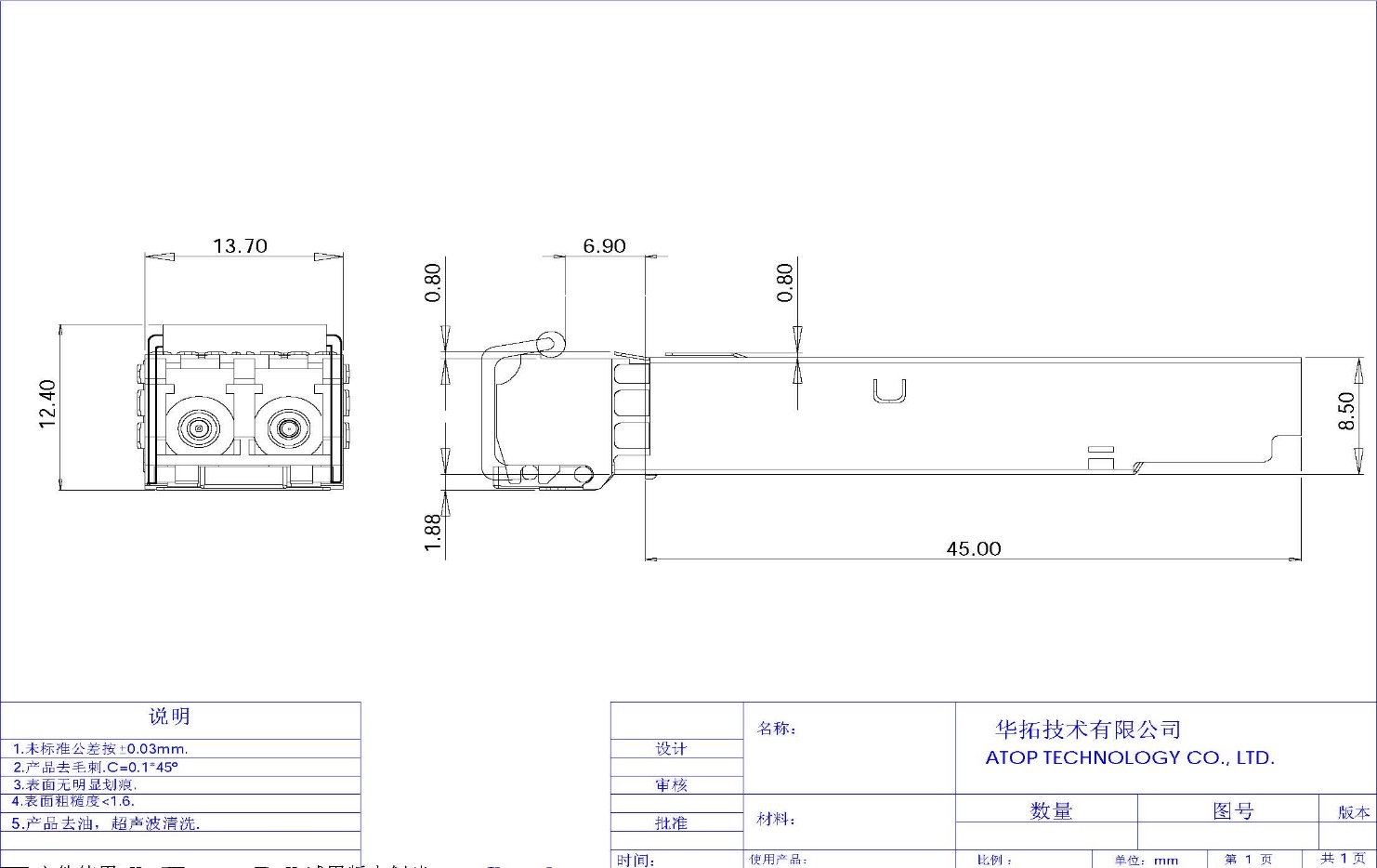
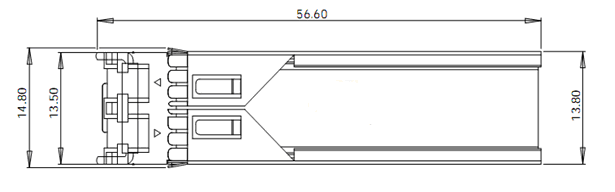
VII. Mechanical Specifications |
Small Form Factor Pluggable (SFP) transceivers are compatible with the dimensions defined by the SFP Multi-Sourcing Agreement (MSA).
.
AP-S85123-3CDLM
|
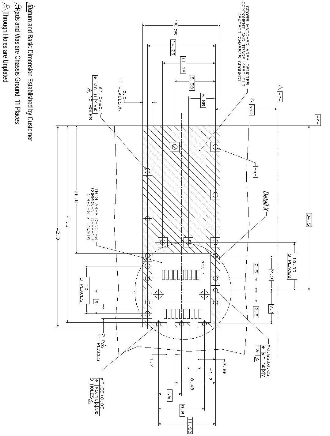
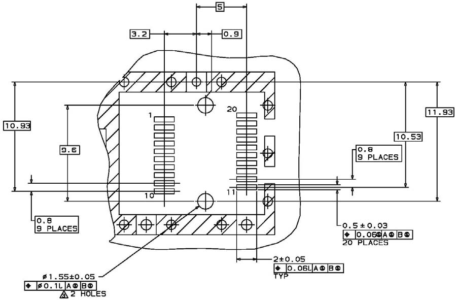
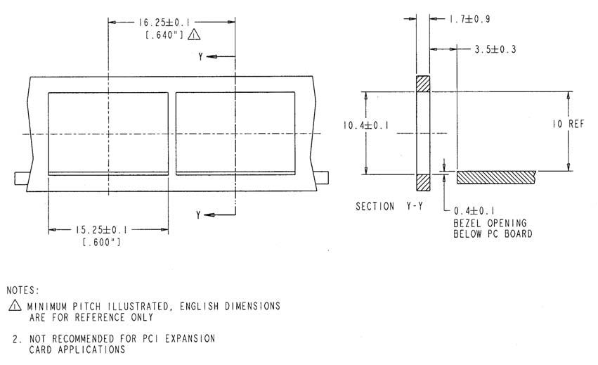
IX. PCB Layout and Bezel Recommendations |