


Dongguan Phynam Comtech Co.,Limited
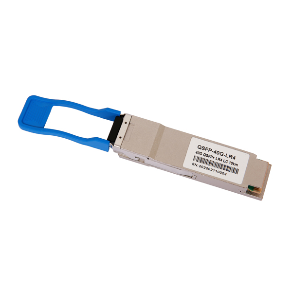
QSFP+/40G-LR4
40Gbps QSFP+ LR4 Transceiver
1 Features
1.1 Duplex LC connector
1.2 Hot-pluggable QSFP+ form factor
1.3 Operating data rate up to11.3Gbps per Lane Up to 10km transmission
1.4 Maximum 3.5W operation power Compliant with IEEE 802.3ba Compliant with SFF 8436
1.5 Digital Diagnostic Monitoring (DDM)
1.6 Complies with RoHS directive (2002/95/EC)
2 Applications
40GBASE-LR4 40G Ethernet
3 General
This product is a high performance 40Gbps transceiver module designed for optical communication applications. It converts 4 channels of 10Gb/s electrical input data to 4 CWDM optical signals, and multiplexes them into a single channel for 40Gb/s optical transmission. On the receiver side, the module optically de-multiplexes a 40Gb/s input into 4 CWDM channels signals, and converts them to 4 channel output electrical data.
4 Performance Specifications
4.1 Absolute Maximum Ratings
|
Parameter |
Symbol |
Min. |
Max. |
Unit |
||||||||||||||
|
Storage Temperature |
Tst |
-40 |
+85 |
°C |
||||||||||||||
|
Operating relative humidity |
RH |
5 |
90 |
% |
||||||||||||||
|
(Non- condensing) |
||||||||||||||||||
|
Input Voltage |
- |
GND |
Vcc |
V |
||||||||||||||
|
Power Supply Voltage |
Vcc |
0 |
3.6 |
V |
||||||||||||||
|
4.2 Recommended Operating Environment |
||||||||||||||||||
|
Parameter |
Symbol |
Min. |
Typ. |
Max. |
Unit |
|||||||||||||
|
Power Supply Voltage |
Vcc |
+3.14 |
+3.3 |
+3.46 |
V |
|||||||||||||
|
Power Supply Current |
Icc |
- |
- |
1130 |
mA |
|||||||||||||
|
Data rate per lane |
- |
10.3125 |
11.3 |
Gbps |
||||||||||||||
|
Operating relative humidity |
RH |
5 |
85 |
% |
||||||||||||||
|
(Non- condensing) |
||||||||||||||||||
|
Case Temperature (Operating) |
TC |
0 |
- |
70 |
°C |
|||||||||||||
|
-40 |
85 |
°C |
||||||||||||||||
|
I2C clock frequency |
- |
- |
100 |
400 |
KHz |
|||||||||||||
|
Power consumption Max |
- |
- |
- |
3.5 |
W |
|||||||||||||
1 / 6

|
4.3 |
Transmitter Characteristics |
||||||||||||||||||||||||||||||
|
Parameter |
Symbol |
Min. |
Typ. |
Max. |
Unit |
Note |
|||||||||||||||||||||||||
|
Signal Speed per lane |
Sp |
10.3125 |
Gbps |
||||||||||||||||||||||||||||
|
1264.5 |
1271 |
1277.5 |
nm |
Lane0 |
|||||||||||||||||||||||||||
|
Center Wavelength |
|
1284.5 |
1291 |
1297.5 |
nm |
Lane1 |
|||||||||||||||||||||||||
|
1304.5 |
1311 |
1317.5 |
nm |
Lane2 |
|||||||||||||||||||||||||||
|
1324.5 |
1331 |
1337.5 |
nm |
Lane3 |
|||||||||||||||||||||||||||
|
Spectral Width (-20dB) |
|
- |
- |
1 |
nm |
||||||||||||||||||||||||||
|
Side Mode Suppression Ratio |
SMSR |
30 |
- |
- |
dB |
||||||||||||||||||||||||||
|
Total Output Optical Power |
Pot |
8.3 |
dBm |
||||||||||||||||||||||||||||
|
Average Optical Output Power |
Po |
-7 |
- |
2.3 |
dBm |
||||||||||||||||||||||||||
|
Optical Modulation Amplitude, |
OMA |
-4 |
3.5 |
dBm |
|||||||||||||||||||||||||||
|
Each Lane |
|||||||||||||||||||||||||||||||
|
Extinction Ratio |
Er |
3.5 |
- |
- |
dB |
||||||||||||||||||||||||||
|
Differential Input Impedance |
- |
80 |
100 |
120 |
Ω |
||||||||||||||||||||||||||
|
Differential Data Input Swing |
VINPP |
120 |
1000 |
mV |
|||||||||||||||||||||||||||
|
4.4 |
Receiver Characteristics |
||||||||||||||||||||||||||||||
|
Parameter |
Symbol |
Min. |
Typ. |
Max. |
Units |
Notes |
|||||||||||||||||||||||||
|
1264.5 |
1271 |
1277.5 |
nm |
Lane0 |
|||||||||||||||||||||||||||
|
Wavelength of Operation |
|
1284.5 |
1291 |
1297.5 |
nm |
Lane1 |
|||||||||||||||||||||||||
|
1304.5 |
1311 |
1317.5 |
nm |
Lane2 |
|||||||||||||||||||||||||||
|
1324.5 |
1331 |
1337.5 |
nm |
Lane3 |
|||||||||||||||||||||||||||
|
Optical Input Power, each lane |
Pin |
-13.7 |
- |
2.3 |
dBm |
||||||||||||||||||||||||||
|
Damage Threshold |
Pmax |
- |
- |
3.3 |
dBm |
4.4.1 |
|||||||||||||||||||||||||
|
Receiver Sensitivity (OMA), each Lane |
Rxsen |
-11.5 |
dBm |
||||||||||||||||||||||||||||
|
Differential Data Output Swing |
VOUTPP |
350 |
800 |
mV |
|||||||||||||||||||||||||||
|
Note4.4.1: Measured with 10.3125Gbps, BER=1x10-12 |
|||||||||||||||||||||||||||||||
|
4.5 Digital Diagnostic Monitoring Characteristics |
|||||||||||||||||||||||||||||||
|
Parameter |
Symbol |
Range |
Accuracy |
||||||||||||||||||||||||||||
|
Transceiver Case |
T |
Measured transceiver case temperature over |
±3°C |
||||||||||||||||||||||||||||
|
Temperature |
specified operating range |
||||||||||||||||||||||||||||||
|
Vcc |
Internally measured transceiver supply |
±3% |
|||||||||||||||||||||||||||||
|
Supply Voltage |
voltage ,3.0~3.6V |
||||||||||||||||||||||||||||||
|
TX Bias Current |
Id |
Measured TX Bias current in uA |
±10% |
||||||||||||||||||||||||||||
|
TX Output Power |
Po |
Measured TX Output Power in dBm Over the |
±3dB |
||||||||||||||||||||||||||||
|
specified output power range |
|||||||||||||||||||||||||||||||
|
Received Optical Power |
Pi |
Measured RX Received Power in dBm Over the |
±3dB |
||||||||||||||||||||||||||||
|
specified input power range |
|||||||||||||||||||||||||||||||
|
5 |
EEPROM Section |
||||||||||||||||||||||||||||||
|
2 / 6 |
|||||||||||||||||||||||||||||||
Compatible with SFF-8436 (QSFP+).
6 Pin Definitions
6.1 Pin Diagram
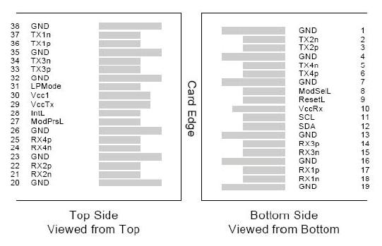
6.2 Pin Descriptions
|
Pin# |
Logic |
Name |
Function |
Notes |
|
|
1 |
GND |
Ground |
|||
|
2 |
CML-I |
Tx2n |
Transmitter Inverted Data Input |
||
|
3 |
CML-I |
Tx2p |
Transmitter Non-Inverted Data output |
||
|
4 |
GND |
Ground |
|||
|
5 |
CML-I |
Tx4n |
Transmitter Inverted Data Input |
||
|
6 |
CML-I |
Tx4p |
Transmitter Non-Inverted Data output |
||
|
7 |
GND |
Ground |
|||
|
8 |
LVTLL-I |
ModSelL |
Module Select |
||
|
9 |
LVTLL-I |
ResetL |
Module Reset |
||
|
10 |
VccRx |
+3.3V Power Supply Receiver |
|||
3 / 6
|
Pin# |
Logic |
Name |
Function |
Notes |
||||||||
|
11 |
SCL |
2-Wire Serial Interface Clock |
||||||||||
|
12 |
SDA |
2-Wire Serial Interface Data |
||||||||||
|
13 |
GND |
Ground |
||||||||||
|
14 |
CML-O |
Rx3p |
Receiver Non-Inverted Data Output |
|||||||||
|
15 |
CML-O |
Rx3n |
Receiver Inverted Data Output |
|||||||||
|
16 |
GND |
Ground |
||||||||||
|
17 |
CML-O |
Rx1p |
Receiver Non-Inverted Data Output |
|||||||||
|
18 |
CML-O |
Rx1n |
Receiver Inverted Data Output |
|||||||||
|
19 |
GND |
Ground |
||||||||||
|
20 |
GND |
Ground |
||||||||||
|
21 |
CML-O |
Rx2n |
Receiver Inverted Data Output |
|||||||||
|
22 |
CML-O |
Rx2p |
Receiver Non-Inverted Data Output |
|||||||||
|
23 |
GND |
Ground |
||||||||||
|
24 |
CML-O |
Rx4n |
Receiver Inverted Data Output |
|||||||||
|
25 |
CML-O |
Rx4p |
Receiver Non-Inverted Data Output |
|||||||||
|
26 |
GND |
Ground |
||||||||||
|
27 |
LVTTL-O |
ModPrsL |
Module Present |
|||||||||
|
28 |
LVTTL-O |
IntL |
Interrupt |
|||||||||
|
29 |
VccTx |
+3.3 V Power Supply transmitter |
||||||||||
|
30 |
Vcc1 |
+3.3 V Power Supply |
||||||||||
4 / 6
|
Pin# |
Logic |
Name |
Function |
Notes |
|||||||
|
31 |
LVTTL-I |
LPMode |
Low Power Mode |
||||||||
|
32 |
GND |
Ground |
|||||||||
|
33 |
CML-I |
Tx3p |
Transmitter Non-Inverted Data Input |
||||||||
|
34 |
CML-I |
Tx3n |
Transmitter Inverted Data Output |
||||||||
|
35 |
GND |
Ground |
|||||||||
|
36 |
CML-I |
Tx1p |
Transmitter Non-Inverted Data Input |
||||||||
|
37 |
CML-I |
Tx1n |
Transmitter Inverted Data Output |
||||||||
|
38 |
GND |
Ground |
|||||||||
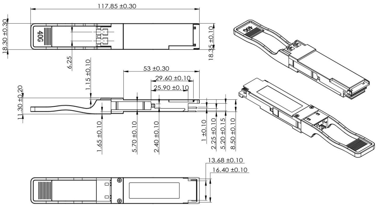
7 Outline Dimensions
8 Ordering Information
|
Part Number |
Operating Case Temperature |
RoHS Compliant |
|
QSFP+/40G-LR4 |
0 ~ 70 °C |
RoHS-6 |
