


Dongguan Phynam Comtech Co.,Limited
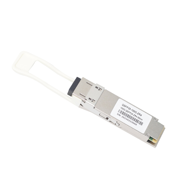
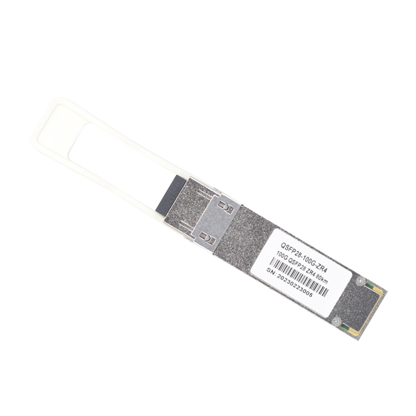
100Gb/s QSFP28 ZR4 Optical Transceiver Module
PHQ28ZR4
Features
Applications
DESCRIPTIONS
This transceiver is designed for 80km optical communication applications. This module contains 4- lane optical transmitter, 4-lane optical receiver and module management block including 2 wire serial inter- face. The optical signals are multiplexed to a single-mode fiber through an industry standard LC connector. A block diagram is shown in Figure 1.
Transceiver Block Diagrams
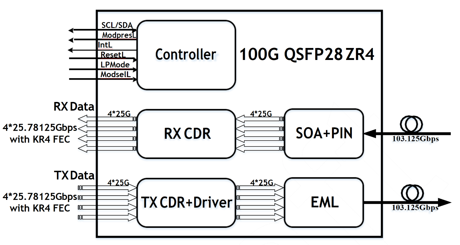
Figure 1. Transceiver Block Diagram
ModSelL:
The ModSelL is an input pin. When held low by the host, the module responds to 2-wire serial communication commands. The ModSelL allows the use of multiple modules on a single 2-wire interface bus. When the Mod- SelL is "High", the module shall not respond to or acknowledge any 2-wire interface communication from the host. ModSelL signal input node shall be biased to the "High" state in the module.
In order to avoid conflicts, the host system shall not attempt 2-wire interface communications within the Mod- SelL de-assert time after any modules are deselected. Similarly, the host shall wait at least for the period of the ModSelL assert time before communicating with the newly selected module. The assertion and de-asserting periods of different modules may overlap as long as the above timing requirements are met.
ResetL :
The ResetL pin shall be pulled to Vcc in the module. A low level on the ResetL pin for longer than the mini- mum pulse length (t_Reset_init) initiates a complete module reset, returning all user module settings to their default state. Module Reset Assert Time (t_init) starts on the rising edge after the low level on the ResetL pin is released. During the execution of a reset (t_init) the host shall disregard all status bits until the module indi- cates a completion of the reset interrupt. The module indicates this by asserting "low" an IntL signal with the Data_Not_Ready bit negated. Note that on power up (including hot insertion) the module should post this completion of reset interrupt without requiring a reset.
LPMode:
The LPMode pin shall be pulled up to Vcc in the module. The pin is a hardware control used to put modules into a low power mode when high. By using the LPMode pin and a combination of the Power override, Power_set and High_Power_Class_Enable software control bits (Address A0h, byte 93 bits 0,1,2).
ModPrsL:
ModPrsL is pulled up to Vcc_Host on the host board and grounded in the module. The ModPrsL is asserted "Low" when inserted and deasserted "High" when the module is physically absent from the host connector. IntL:
IntL is an output pin. When IntL is "Low", it indicates a possible module operational fault or a status critical to the host system. The host identifies the source of the interrupt using the 2-wire serial interface. The IntL pin is an open collector output and shall be pulled to host supply voltage on the host board. The INTL pin is deas- serted "High" after completion of reset, when byte 2 bit 0 (Data Not Ready) is read with a value of '0' and the flag field is read (see SFF-8636).
Pin Descriptions
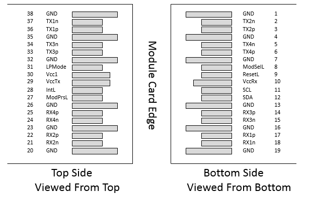 Figure 2. MSA compliant Connector
|
Pin |
Symbol |
Description |
Notes |
|
1 |
GND |
Ground |
1 |
|
2 |
Tx2n |
Transmitter Inverted Data Input |
|
|
3 |
Tx2p |
Transmitter Non-Inverted Data Input |
|
|
4 |
GND |
Ground |
1 |
|
5 |
Tx4n |
Transmitter Inverted Data Input |
|
|
6 |
Tx4p |
Transmitter Non-Inverted Data Input |
|
|
7 |
GND |
Ground |
1 |
|
8 |
ModSelL |
Module Select |
|
|
9 |
ResetL |
Module Reset |
|
|
10 |
Vcc Rx |
+3.3V Power Supply Receiver |
|
|
11 |
SCL |
2-wire serial interface clock |
|
|
12 |
SDA |
2-wire serial interface data |
|
|
13 |
GND |
Ground |
1 |
|
14 |
Rx3p |
Receiver Non-Inverted Data Output |
|
|
15 |
Rx3n |
Receiver Inverted Data Output |
|
|
16 |
GND |
Ground |
1 |
|
17 |
Rx1p |
Receiver Non-Inverted Data Output |
|
|
18 |
Rx1n |
Receiver Inverted Data Output |
|
|
19 |
GND |
Ground |
1 |
|
20 |
GND |
Ground |
1 |
|
21 |
Rx2n |
Receiver Inverted Data Output |
|
|
22 |
Rx2p |
Receiver Non-Inverted Data Output |
|
|
23 |
GND |
Ground |
1 |
|
24 |
Rx4n |
Receiver Non-Inverted Data Output |
|
|
25 |
Rx4p |
Receiver Inverted Data Output |
|
|
26 |
GND |
Ground |
1 |
|
27 |
ModPrsL |
Module Present |
|
|
28 |
IntL |
Interrupt |
|
|
29 |
Vcc Tx |
+3.3V Power supply transmitter |
|
|
30 |
Vcc1 |
+3.3V Power supply |
|
|
31 |
LPMode |
Low Power Mode |
|
|
32 |
GND |
Ground |
1 |
|
33 |
Tx3p |
Transmitter Non-Inverted Data Input |
|
|
34 |
Tx3n |
Transmitter Inverted Data Input |
|
|
35 |
GND |
Ground |
1 |
|
36 |
Tx1p |
Transmitter Non-Inverted Data Input |
|
|
37 |
Tx1n |
Transmitter Inverted Data Input |
|
|
38 |
GND |
Ground |
1 |
Notes
1.Circuit ground is internally isolated from chassis ground.
Absolute Maximum Ratings
It has to be noted that the operation in excess of any individual absolute maximum ratings might cause perma- nent damage to this module.
|
Parameter |
Symbol |
Min |
Typ |
Max |
Unit |
Notes |
|
Maximum Supply Voltage |
Vcc |
0 |
3.6 |
V |
||
|
Storage Temperature |
Ts |
-40 |
85 |
℃ |
||
|
Relative Humidity |
RH |
15 |
85 |
% |
1 |
|
|
Damage Threshold, each lane |
THd |
6.5 |
dBm |
Notes
1. Non-condensing
Operating Environments
Electrical and optical characteristics below are defined under this operating environment, unless otherwise specified.
|
Parameter |
Symbol |
Min |
Typ |
Max |
Unit |
|
Supply Voltage |
Vcc |
3.135 |
3.3 |
3.465 |
V |
|
Case Temperature |
Top |
0 |
70 |
℃ |
|
|
Link Distance with G.652 |
80 |
km |
Electrical Characteristics
|
Parameter |
Symbol |
Min |
Typ |
Max |
Unit |
Note |
|
Power dissipation |
6.5 |
W |
||||
|
Supply Current |
Icc |
1.8759 |
A |
Steady state |
||
|
Transmitter |
||||||
|
Data Rate, each lane |
25.78125 |
Gbps |
||||
|
Differential Voltage pk-pk |
Vpp |
900 |
mV |
At 1 MHz |
||
|
Common Mode Voltage |
Vcm |
-350 |
2850 |
mV |
||
|
Transition time |
Trise/Tfall |
10 |
ps |
20%~80% |
||
|
Differential Termination Resistance Mismatch |
10 |
% |
||||
|
Eye width |
EW15 |
0.46 |
UI |
|||
|
Eye height |
EH15 |
95 |
mV |
|||
|
Receiver |
||||||
|
Data Rate, each lane |
25.78125 |
Gbps |
||||
|
Differential Termination Resistance Mismatch |
10 |
% |
At 1 MHz |
|||
|
Differential output voltage swing |
Vout, pp |
900 |
mV |
|||
|
Common Mode Noise, RMS |
Vrms |
17.5 |
mV |
|||
|
Transition time |
Trise/Tfall |
12 |
ps |
20%~80% |
||
|
Eye width |
EW15 |
0.57 |
UI |
|||
|
Eye height |
EH15 |
228 |
mV |
|||
Optical Characteristics
100GBASE-ZR4 Operation(EOL, TOP = 0 to +70 ℃ , VCC = 3.135 to 3.465 Volts)
|
Parameters |
Unit |
min |
type |
max |
Note |
|
Transmitter |
|||||
|
Signaling Speed per Lane |
Gb/s |
25.78125 ± 100 ppm |
|||
|
Transmit wavelengths |
nm |
1294.53 |
1296.59 |
||
|
1299.02 |
1301.09 |
||||
|
1303.54 |
1305.63 |
||||
|
1308.09 |
1310.19 |
||||
|
Side-Mode Suppression Ratio (SMSR) |
dB |
30 |
|||
|
Total Average Launch Power |
dBm |
8 |
12.5 |
||
|
Average launch power, each lane |
dBm |
2 |
6.5 |
||
|
Difference in launch power between any two lanes(Average and OMA) |
dBm |
3 |
|||
|
Average launch power of OFF transmitter, each lane |
dBm |
-30 |
|||
|
Extinction Ratio (ER) |
dB |
6 |
|||
|
RIN OMA |
dB/Hz |
-130 |
|||
|
Optical return loss tolerance |
dB |
20 |
|||
|
Transmitter reflectance |
dB |
-12 |
|||
|
Transmitter eye mask definition {X1, X2, X3, Y1, Y2, Y3} |
{0.25, 0.4, 0.45, 0.25, 0.28, 0.4} |
1 |
|||
|
Mask margin |
% |
5 |
|||
|
Receiver |
|||||
|
Signaling Speed per Lane |
Gb/s |
25.78125 ± 100 ppm |
|||
|
Receive wavelengths |
nm |
1294.53 |
1296.59 |
||
|
1299.02 |
1301.09 |
||||
|
1303.54 |
1305.63 |
||||
|
1308.09 |
1310.19 |
||||
|
Average receiver power, each lane |
dBm |
-28 |
-7 |
||
|
Receiver power, each lane(OMA) |
dBm |
-7 |
|||
|
Receiver reflectance |
dB |
-26 |
|||
|
Receiver sensitivity Average, each lane |
dBm |
-28 |
1 |
||
|
Receiver 3 dB electrical upper cutoff frequency, each lane |
GHz |
31 |
|||
|
Damage threshold, each lane |
dBm |
6.5 |
|||
|
LOS Assert |
dBm |
-40 |
|||
|
LOS Deassert |
dBm |
-29 |
|||
|
LOS Hysteresis |
dB |
0.5 |
|||
Notes
EEPROM Definitions
Lower Memory Map
|
Address |
Type |
Size |
Name |
Description |
Value(Hex) |
Remarks |
|
0 |
R |
1 |
Identifier |
Identifier |
||
|
1 |
R |
1 |
Status |
Revision Compliance |
||
|
2 |
R |
1 |
Status |
Flat_mem/ IntL/Data_Not_Ready |
||
|
3 |
R |
1 |
Interrupt Flags |
Latched TX/RX LOS indicator |
||
|
4 |
R |
1 |
Latched TX Adaptive EQ/TX Transmit-ter/Laser fault indicator |
|||
|
5 |
R |
1 |
Latched TX/RX CDR LOL indicator |
|||
|
6 |
R |
1 |
Latched temperature A/W / Initialization complete flag |
|||
|
7 |
R |
1 |
Latched supply voltage A/W |
|||
|
8 |
R |
1 |
Vendor Specific |
|||
|
9~10 |
R |
2 |
Latched RX power A/W |
|||
|
11~12 |
R |
2 |
Latched TX bias A/W |
|||
|
13~14 |
R |
2 |
Latched TX power A/W |
|||
|
15~18 |
R |
4 |
Reserved |
|||
|
19-21 |
R |
2 |
Vendor Specific |
|||
|
22-23 |
R |
2 |
Device moniors |
Module temperature |
||
|
24-25 |
R |
2 |
Reserved |
|||
|
26-27 |
R |
2 |
Supply voltage |
|||
|
28-29 |
R |
2 |
Reserved |
|||
|
30-33 |
R |
4 |
Vendor Specific |
|||
|
34-35 |
R |
2 |
Power moniors |
RX input power, channel 1 |
||
|
36-37 |
R |
2 |
RX input power, channel 2 |
|||
|
38-39 |
R |
2 |
RX input power, channel 3 |
|||
|
40-41 |
R |
2 |
RX input power, channel 4 |
|||
|
42-43 |
R |
2 |
LD Bias Monitors |
TX bias, channel 1 |
||
|
44-45 |
R |
2 |
TX bias, channel 2 |
|||
|
46-47 |
R |
2 |
TX bias, channel 3 |
|||
|
48-49 |
R |
2 |
TX bias, channel 4 |
|||
|
50-51 |
R |
2 |
Power monitors |
TX power, channel 1 |
||
|
52-53 |
R |
2 |
TX power, channel 2 |
|||
|
54-55 |
R |
2 |
TX power, channel 3 |
|||
|
56-57 |
R |
2 |
TX power, channel 4 |
|||
|
58-73 |
R |
16 |
Reserved |
|||
|
74-81 |
R |
8 |
Vendor Specific |
|||
|
82-85 |
R |
4 |
Reserved |
|||
|
86 |
RW |
1 |
Control |
Tx Disable |
||
|
87 |
RW |
1 |
Rx_Rate_select |
|||
|
88 |
RW |
1 |
Tx _Rate_select |
|||
|
89~92 |
RW |
4 |
Rx_Application_Select |
|||
|
93 |
RW |
1 |
Power |
|||
|
94~97 |
RW |
4 |
Tx_Application_Select |
|||
|
98 |
RW |
1 |
TX/RX CDR_control |
|||
|
99 |
RW |
1 |
Reserved |
|||
|
100-104 |
RW |
4 |
Free Side De- vice and Channel Masks |
Module and Channel Masks |
||
|
105 |
RW |
1 |
Vendor Specific |
|||
|
106 |
RW |
1 |
Vendor Specific |
|||
|
107 |
RW |
1 |
Reserved |
|||
|
108-109 |
R |
2 |
Free Side Device Properties |
Most significant byte of propagation delay |
||
|
110 |
R |
1 |
Advanced Low Power Mode / Far Side Managed / Min Operating Voltage |
|||
|
111-112 |
RW |
2 |
Assigned for use by PCI Express |
PCI |
||
|
113 |
R |
1 |
Free Side Device Properties |
End Implementation |
||
|
114-118 |
RW |
6 |
Reserved |
|||
|
119-122 |
W |
4 |
Password Change Entry Area |
|||
|
123-126 |
W |
4 |
Password Entry Area |
|||
|
127 |
RW |
1 |
Page Select Byte |
Upper Memory Map Page 00h
|
Address |
Type |
Size |
Name |
Description |
Value(Hex) |
Remarks |
|
128 |
R |
1 |
Identifier |
Identifier Type of serial Module |
||
|
129 |
R |
1 |
Ext. Identifier |
Extended Identifier to free side device. Includes power classes, CLEI codes, CDR capability |
||
|
130 |
R |
1 |
Connector |
Code for connector type |
||
|
131 |
R |
1 |
Specification compliance |
10/40G/100G Ethernet Compliance |
||
|
132 |
R |
1 |
SONET Compliance Codes |
|||
|
133 |
R |
1 |
SAS/SATA Compliance Codes |
|||
|
134 |
R |
1 |
Gigabit Ethernet Compliant Codes |
|||
|
135~136 |
R |
1 |
Fibre Channel link length/Fibre Channel Transmitter Technology |
|||
|
137 |
R |
1 |
Fibre Channel transmission media |
|||
|
138 |
R |
1 |
Fibre Channel Speed |
|||
|
139 |
R |
1 |
Encoding |
Code for serial encoding algorithm. |
||
|
140 |
R |
1 |
Nominal bit rate, units of 100Mbps. For BR>25.4G, set this to FFh and use Byte 222 |
|||
|
141 |
R |
1 |
QSFP+ Rate Select Version 2. |
|||
|
142 |
R |
1 |
Link length supported for SMF fiber in km. |
|||
|
143 |
R |
1 |
Length |
Length(OM3 50 um) |
||
|
144 |
R |
1 |
Length(OM2 50 um) |
|||
|
145 |
R |
1 |
Length(OM1 62.5 um) |
|||
|
146 |
R |
1 |
Length(OM5 50um) |
|||
|
147 |
R |
1 |
Device technology |
Device technology |
||
|
148 |
R |
1 |
Vendor name |
Free side device vendor |
||
|
149 |
R |
1 |
||||
|
150 |
R |
1 |
||||
|
151 |
R |
1 |
||||
|
152 |
R |
1 |
||||
|
153 |
R |
1 |
||||
|
154 |
R |
1 |
||||
|
155 |
R |
1 |
||||
|
156 |
R |
1 |
||||
|
157 |
R |
1 |
||||
|
158 |
R |
1 |
||||
|
159 |
R |
1 |
||||
|
160 |
R |
1 |
||||
|
161 |
R |
1 |
||||
|
162 |
R |
1 |
||||
|
163 |
R |
1 |
||||
|
164 |
R |
1 |
Extended Module |
|||
|
165~167 |
R |
1 |
Vendor OUI |
|||
|
168 |
R |
1 |
Vendor PN |
Part number provided by free side device vendor |
||
|
169 |
R |
1 |
||||
|
170 |
R |
1 |
||||
|
171 |
R |
1 |
||||
|
172 |
R |
1 |
||||
|
173 |
R |
1 |
||||
|
174 |
R |
1 |
||||
|
175 |
R |
1 |
||||
|
176 |
R |
1 |
||||
|
177 |
R |
1 |
||||
|
178 |
R |
1 |
||||
|
179 |
R |
1 |
||||
|
180 |
R |
1 |
||||
|
181 |
R |
1 |
||||
|
182 |
R |
1 |
||||
|
183 |
R |
1 |
||||
|
184 |
R |
1 |
Vendor rev |
Revision level for part number provided by vendor |
||
|
185 |
R |
1 |
||||
|
186 |
R |
1 |
Wavelength |
Nominal laser wavelength (wave- length=value/20 in nm) |
||
|
187 |
R |
1 |
||||
|
188 |
R |
1 |
Wavelength tolerance |
Guaranteed range of laser wave- length(+/- value) from nominal wave- length. (wavelength Tol.=value/200 in nm) |
||
|
189 |
R |
1 |
||||
|
190 |
R |
1 |
Max case temp |
Maximum case temperature in degrees C |
||
|
191 |
R |
1 |
C_BASE |
Check code for base ID fields |
||
|
192 |
R |
1 |
Link codes |
Extended Specification Compliance Codes |
||
|
193 |
R |
1 |
Options |
TX Input Equalization Auto Adaptive Capable not implemented, TX Input Equalization Fixed Program- mable Settings implemented, RX Output Emphasis Fixed Programma- ble Settings implemented, RX Output Amplitude Fixed Programmable Settings implemented |
||
|
194 |
R |
1 |
Tx CDR LOL Flag, Rx CDR LOL Flag, RX Squelch Disable, RX Output Disable,TX Squelch Disable, TX Squelch |
|||
|
195 |
R |
1 |
Memory page 02h implemented, Memory page 01h implemented, Active control of the select bits in the up- per memory table is required to change rates, Tx_DISABLE and serial output imple- mented, Tx_FAULT signal implemented, Tx Loss of Signal implemented |
|||
|
196 |
R |
1 |
Vendor SN |
Serial number provided by vendor |
||
|
197 |
R |
1 |
||||
|
198 |
R |
1 |
||||
|
199 |
R |
1 |
||||
|
200 |
R |
1 |
||||
|
201 |
R |
1 |
||||
|
202 |
R |
1 |
||||
|
203 |
R |
1 |
||||
|
204 |
R |
1 |
||||
|
205 |
R |
1 |
||||
|
206 |
R |
1 |
||||
|
207 |
R |
1 |
||||
|
208 |
R |
1 |
||||
|
209 |
R |
1 |
||||
|
210 |
R |
1 |
||||
|
211 |
R |
1 |
||||
|
212 |
R |
1 |
Date Code |
Vendor's manufacturing date code |
||
|
213 |
R |
1 |
||||
|
214 |
R |
1 |
||||
|
215 |
R |
1 |
||||
|
216 |
R |
1 |
||||
|
217 |
R |
1 |
||||
|
218 |
R |
1 |
||||
|
219 |
R |
1 |
||||
|
220 |
R |
1 |
Monitoring Type Diagnostic |
Average RX power measurement, Transmitter power measurement supported |
||
|
221 |
R |
1 |
Enhanced Options |
Indicates which optional enhanced fea- tures are implemented (if any) in the free side device. |
||
|
222 |
R |
1 |
BR, nominal |
Nominal bit rate per channel, units of 250Mbps. |
||
|
223 |
R |
1 |
CC_EXT |
Check Code for Address 192 to 222 |
||
|
224 |
R |
1 |
Vendor Specific |
|||
|
225 |
R |
1 |
||||
|
226 |
R |
1 |
||||
|
227 |
R |
1 |
||||
|
228 |
R |
1 |
||||
|
229 |
R |
1 |
||||
|
230 |
R |
1 |
||||
|
231 |
R |
1 |
||||
|
232 |
R |
1 |
||||
|
233 |
R |
1 |
||||
|
234 |
R |
1 |
||||
|
235 |
R |
1 |
||||
|
236 |
R |
1 |
||||
|
237 |
R |
1 |
||||
|
238 |
R |
1 |
||||
|
239 |
R |
1 |
||||
|
240 |
R |
1 |
Vendor Spe- cific |
|||
|
241 |
R |
1 |
||||
|
242 |
R |
1 |
Vendor Specific |
|||
|
243 |
R |
1 |
Reserved |
|||
|
244 |
R |
1 |
||||
|
245 |
R |
1 |
||||
|
246 |
R |
1 |
||||
|
247 |
R |
1 |
||||
|
248 |
R |
1 |
||||
|
249 |
R |
1 |
||||
|
250 |
R |
1 |
Checksum |
|||
|
251 |
R |
1 |
Vendor Specific |
|||
|
252 |
R |
1 |
||||
|
253 |
R |
1 |
||||
|
254 |
R |
1 |
||||
|
255 |
R |
1 |
Digital Diagnostic Monitoring Functions
This transceiver support the I2C-based Diagnostic Monitoring Interface (DMI) defined in document SFF- 8636. The host can access real-time performance of transmitter and receiver optical power, temperature, sup- ply voltage and bias current.
|
Performance Item |
Related Bytes(A0[00] memory) |
Monitor Error |
Notes |
|
Module temperature |
22 to 23 |
+/-3°C |
1,2 |
|
Module voltage |
26 to 27 |
< 3% |
2 |
|
LD Bias current |
42 to 49 |
< 10% |
2 |
|
Transmitter optical power |
50 to 57 |
< 3dB |
2 |
|
Receiver optical power |
34 to 41 |
< 4dB |
2 |
Note
Alarm and Warning Thresholds
This transceiver support alarms function, indicating the values of the preceding basic performance are lower or higher than the thresholds.
|
Performance Item |
Alarm Threshold Bytes(A0[03] memory) |
Unit |
Low threshold |
High threshold |
|
Temp Alarm |
128 to 131 |
℃ |
-10 |
80 |
|
Temp Warning |
132 to 135 |
℃ |
0 |
70 |
|
Voltage Alarm |
144 to 147 |
V |
2.97 |
3.63 |
|
Voltage Warning |
148 to 151 |
V |
3.135 |
3.465 |
|
TX Power Alarm |
192 to 195 |
dBm |
-4 |
8.2 |
|
TX Power Warning |
196 to 199 |
dBm |
-1 |
6.5 |
|
RX Power Alarm |
176 to 179 |
dBm |
-31 |
-4 |
|
RX Power Warning |
180 to 183 |
dBm |
-28 |
-7 |
Mechanical Specifications
This 100G ZR4 QSFP28 transceivers are compatible with the QSFP28 Specification for pluggable form factor modules.
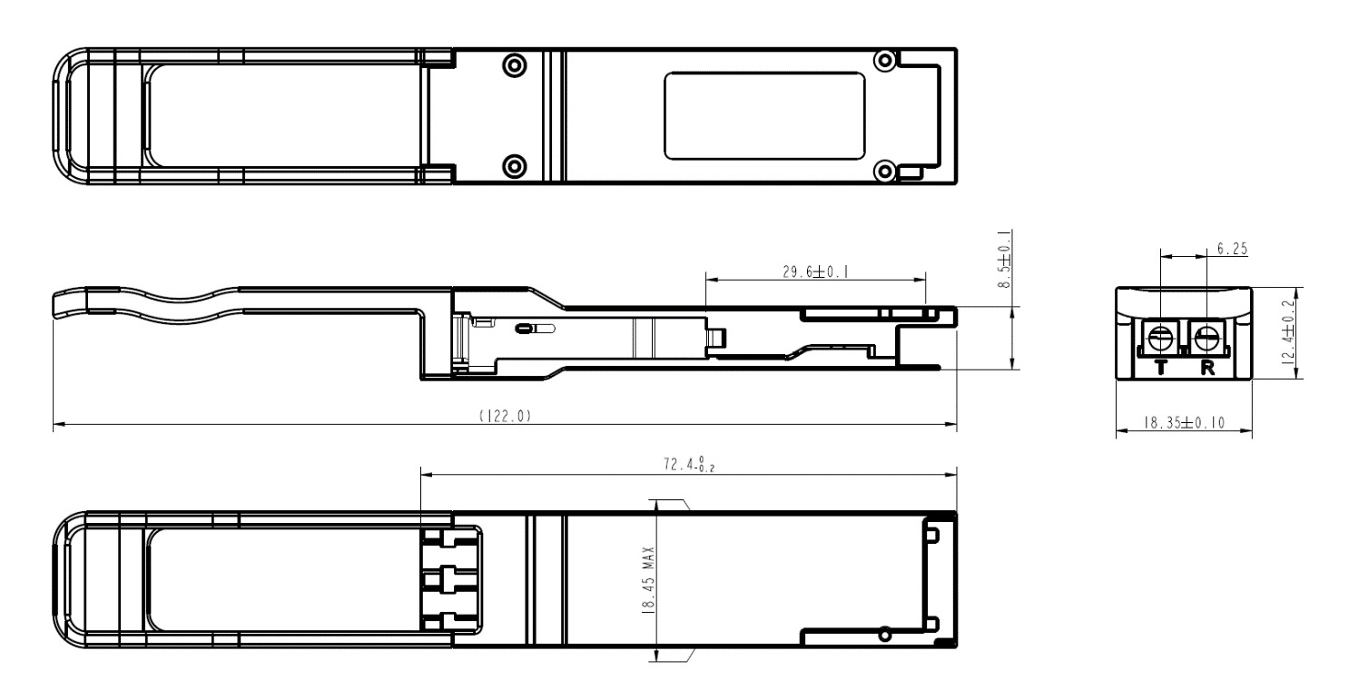
Figure 3. Mechanical Dimensions
Regulatory Compliance
|
Feature |
Standard |
Performance |
|
Safety |
||
|
NRTL |
UL 62368-1:2014 |
UL recognized component for US and CAN |
|
CAN/CSA C22.2 No. 62368-1-14 |
||
|
IEC 60825-1:2014 |
||
|
IEC 60825-2:2014+A1:2007+A2:2010 |
||
|
TUV |
EN 62368-1:2014+A11:2017(Second Edition) |
TUV certificate |
|
EN 60825-1:2014 |
||
|
EN 60825-1:2014+A1:2007+A2:2010 |
||
|
IEC 62368-1:2014(Second Edition) |
||
|
FDA |
U.S. 21 CFR 1040.10 |
FDA/CDRH certified with acces-sion number according to Laser Notice 50 |
|
Electromagnetic Compatibility |
||
|
Radiated emissions |
EMC Directive 2014/30/EU |
Class B digital device with a mini- mum -6dB margin to the limit when tested with a metal enclo-sure. Final margin may vary de-pending on sys- tem application, good system EMI de- sign practice, ie: suitable metal enclo- sure and well-bonding, is required to achieve Class B margins at the system level. Tested frequency range: 30 MHz to 40 GHz or 5th harmonic (5 times the highest frequency), whichever is less. |
|
EN 55032 |
||
|
CISPR 32 |
||
|
FCC rules 47 CFR Part 15 |
||
|
ICES-003 |
||
|
AS/NZS CISPR 32 |
||
|
ESD |
EN 55024 |
Withstands discharges of ± 8 k V contact, ±15 k V air. |
|
CISPR 24 |
||
|
IEC/EN 61000-4-2 |
||
|
Radiated immunity |
EN 55035 |
Field strength of 10 V/m from 80 MHz to 6 GHz. |
|
CISPR 35 |
||
|
IEC/EN 61000-4-3 |
||
|
Restriction of Hazardous Substances |
||
|
RoHS |
EU Directive 2011/65/EU (EU) 2015/863 |
|
ESD Design
Normal ESD precautions are required during the handling of this module. This transceiver is shipped in ESD protective packaging. It should be removed from the packaging and otherwise handled in an ESD protected environment utilizing standard grounded benches, floor mats, and wrist straps.
|
Parameter |
Threshold value |
Notes |
|
ESD of high-speed pins |
1KV |
Human Body Model |
|
ESD of low-speed pins |
2KV |
Human Body Model |
|
Air discharge during operation |
15KV |
|
|
Direct contact discharges to the case |
8KV |
