


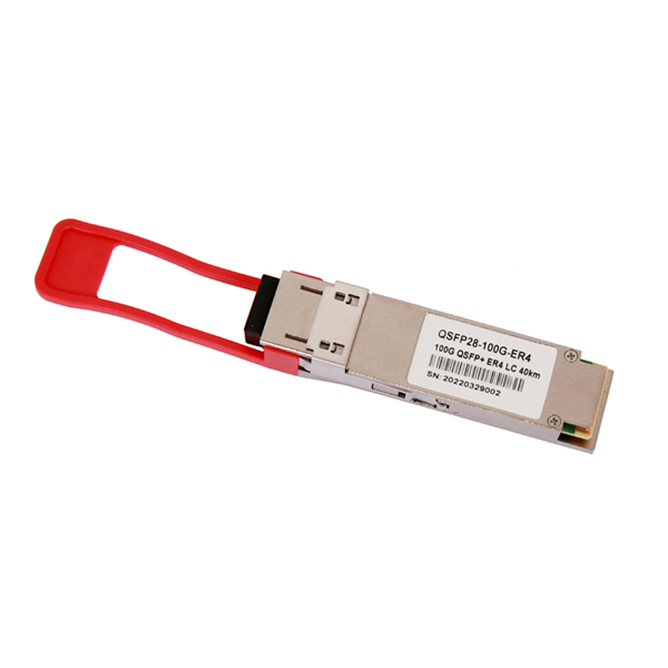

Dongguan Phynam Comtech Co.,Limited
100Gb/s QSFP28 ER4 & 100GBASE-ER4 Lite Optical Transceiver Module
PH-QSFP28/100G-ER4 & PH-QSFP28/100G-ER4L
Features
Applications
Parameter
|
Parameter |
Symbol |
Min. |
Typical |
Max. |
Unit |
Notes |
|
Storage Temperature |
TS |
-40 |
- |
85 |
ºC |
|
|
Supply Voltage |
VCC |
-0.5 |
- |
3.6 |
V |
|
|
Relative Humidity (non-condensing) |
RH |
5 |
- |
95 |
% |
|
|
Data Input Voltage – Differential |
lVDIP-VDINl |
- |
- |
1 |
V |
|
|
Control Input Voltage |
VI |
-0.3 |
- |
Vcc+0.5 |
V |
|
|
Control Output Current |
IO |
-20 |
- |
20 |
mA |
Recommended Operating Conditions
|
Parameter |
Symbol |
Min. |
Typical |
Max. |
Unit |
Notes |
|
Operating Case Temperature |
TOPR |
0 |
- |
70 |
ºC |
|
|
Power Supply Voltage |
VCC |
3.135 |
3.3 |
3.465 |
V |
|
|
Instantaneous peak current at hot plug |
ICC_IP |
- |
- |
1800 |
mA |
|
|
Sustained peak current at hot plug |
ICC_SP |
- |
- |
1485 |
mA |
|
|
Maximum Power Dissipation |
PD |
- |
- |
4.5 |
W |
|
|
Maximum Power Dissipation, Low Power Mode |
PDLP |
- |
- |
1.5 |
W |
|
|
Aggregate Bit Rate |
ABR |
- |
103.125 |
- |
Gb/s |
|
|
Data Rate per Lane |
DRL |
- |
25.78 |
- |
Gb/s |
|
|
Control Input Voltage High |
VIH |
VCC*0.7 |
- |
VCC+0.3 |
V |
|
|
Control Input Voltage Low |
VIL |
-0.3 |
- |
VCC*0.3 |
V |
|
|
Two Wire Serial Interface Clock Rate |
- |
- |
- |
400 |
kHz |
|
|
Power Supply Noise Tolerance |
- |
- |
- |
66 |
mVpp |
10 Hz -10 MHz |
|
Rx Differential Data Output Load |
- |
- |
100 |
- |
ohms |
|
|
Operating Distance |
- |
2 |
- |
40,000 |
m |
With FEC |
Transmitter Optical Specifications
|
Parameter |
Symbol |
Min. |
Typical |
Max. |
Unit |
Notes |
|
Wavelength L0 |
λC0 |
1294.53 |
1295.56 |
1296.59 |
nm |
|
|
Wavelength L1 |
λC1 |
1299.02 |
1300.05 |
1301.09 |
nm |
|
|
Wavelength L2 |
λC2 |
1303.54 |
1304.58 |
1305.63 |
nm |
|
|
Wavelength L3 |
λC3 |
1308.09 |
1309.14 |
1310.19 |
nm |
|
|
Side-mode suppression ratio |
SMSR |
30 |
dB |
|||
|
Total Average Optical Launch Power |
POUT |
- |
- |
12.5 |
dBm |
|
|
Average Launch Power Tx_Off (Each Lane) |
POUT_OFF |
- |
- |
-30 |
dBm |
|
|
Average Optical Launch Power (Each Lane) |
POUTL |
-2.5 |
- |
6.5 |
dBm |
|
|
Extinction Ratio |
ER |
4.5 |
- |
- |
dB |
|
|
Optical Modulation Amplitude (OMA), (Each Lane) |
OMA |
0.5 |
- |
6.5 |
dBm |
|
|
Launch Power in OMA minus TDP (Each Lane) |
OMA-TDP |
-0.5 |
- |
- |
dBm |
|
|
Difference in launch power between any two lanes (Average and OMA) |
DT_OMA |
- |
- |
4 |
dB |
|
|
Transmitter and Dispersion Penalty (Each Lane) |
TDP |
- |
- |
3 |
dB |
|
|
Optical Return Loss Tolerance |
ORLT |
20 |
- |
- |
dB |
|
|
Transmitter Eye Mask Definition |
- |
{0.25, 0.4, 0.45, 0.25, 0.28, 0.4} |
||||
|
Transmitter Reflectance |
TR |
- |
- |
-26 |
dB |
|
Receiver Optical Specifications
|
Parameter |
Symbol |
Min. |
Typical |
Max. |
Unit |
Notes |
|
Wavelength L0 |
λC0 |
1294.53 |
1295.56 |
1296.59 |
nm |
|
|
Wavelength L1 |
λC1 |
1299.02 |
1300.05 |
1301.09 |
nm |
|
|
Wavelength L2 |
λC2 |
1303.54 |
1304.58 |
1305.63 |
nm |
|
|
Wavelength L3 |
λC3 |
1308.09 |
1309.14 |
1310.19 |
nm |
|
|
Receiver sensitivity (OMA), each lane at 5 x 10⁻⁵ BER |
- |
- |
-18.5 |
dBm |
||
|
Stressed receiver sensitivity (OMA), each lane |
- |
- |
- |
-16 |
dBm |
|
|
Stressed Receiver Sensitivity Test Conditions: |
||||||
|
Stressed Eye J2 Jitter (Each Lane) |
- |
- |
0.33 |
- |
UI |
|
|
Stressed Eye J4 Jitter (Each Lane) |
- |
- |
0.48 |
- |
UI |
|
|
Vertical Eye Closure Penalty |
- |
- |
2.5 |
- |
dB |
|
|
SRS eye mask definition { X1, X2, X3, Y1, Y2, Y3} |
(0.39, 0.5, 0.5, 0.39, 0.39, 0.4) |
|||||
|
Damage threshold, each lane |
Pin, damage |
-2.5 |
- |
- |
dBm |
|
|
Average Receive Power (Each Lane) |
- |
-20.5 |
- |
-3.5 |
dBm |
|
|
Receive Power in OMA (Each Lane), Overload |
OMA |
- |
- |
-3.5 |
dBm |
|
|
Receiver Reflectance |
RXR |
- |
- |
-26 |
dB |
|
Electrical Specifications
High-Speed Signal:Compliant to CAUI-4 (IEEE 802.3bm)
Low-Speed Signal: Compliant to SFF-8679
|
Transmitter (Module Input) |
||||||
|
Parameter |
Symbol |
Min. |
Typical |
Max. |
Unit |
Notes |
|
Differential Data Input Amplitude |
VIN,P-P |
95 |
- |
900 |
mVpp |
Note 1 |
|
Differential Termination Mismatch |
- |
- |
10 |
% |
||
|
LPMode, Reset and ModSelL |
VIL |
-0.3 |
- |
0.8 |
V |
|
|
VIH |
2 |
- |
VCC+0.3 |
V |
||
|
Receiver (Module Output) |
||||||
|
Parameter |
Symbol |
Min. |
Typical |
Max. |
Unit |
Notes |
|
Differential Data Output Amplitude |
VOUT,P-P |
250 |
- |
900 |
mVpp |
Note 1 |
|
Differential Termination Mismatch |
- |
- |
10 |
% |
||
|
Output Rise/Fall Time, 20%~80% |
TR |
9.5 |
- |
- |
ps |
|
|
ModPrsL and IntL |
VOL |
0 |
- |
0.4 |
V |
IOL=4mA |
|
VOH |
VCC-0.5 |
- |
VCC+0.3 |
V |
IOL=-4mA |
|
I/O Timing for Squelch & Disable
|
Parameter |
Symbol |
Min. |
Typical |
Max. |
Unit |
Notes |
|
Rx Squelch Assert Time |
ton_Rxsq |
80 |
µs |
|||
|
Rx Squelch Deassert Time |
toff_Rxsq |
80 |
µs |
|||
|
Tx Squelch Assert Time |
ton_Txsq |
400 |
ms |
|||
|
Tx Squelch Deassert Time |
toff_Txsq |
400 |
ms |
|||
|
Tx Disable Assert Time |
ton_txdis |
100 |
ms |
|||
|
Tx Disable Deassert Time |
toff_txdis |
400 |
ms |
|||
|
Rx Output Disable Assert Time |
ton_rxdis |
100 |
ms |
|||
|
Rx Output Disable Deassert Time |
toff_rxdis |
100 |
ms |
|||
|
Squelch Disable Assert Time |
ton_sqdis |
100 |
ms |
|||
|
Squelch Disable Deassert Time |
toff_sqdis |
100 |
ms |
Digital Diagnostics
|
Parameter |
Range |
Accuracy |
Unit |
Calibration |
|
Temperature |
0 to 70 |
±3 |
ºC |
Internal |
|
Voltage |
0 to VCC |
0.1 |
V |
Internal |
|
Tx Bias Current (Each Lane) |
0 to 100 |
10% |
mA |
Internal |
|
Tx Output Power (Each Lane) |
-2.5 to 6.5 |
±3 |
dB |
Internal |
|
Rx Power (Each Lane) |
-20.5 to -3.5 |
±3 |
dB |
Internal |
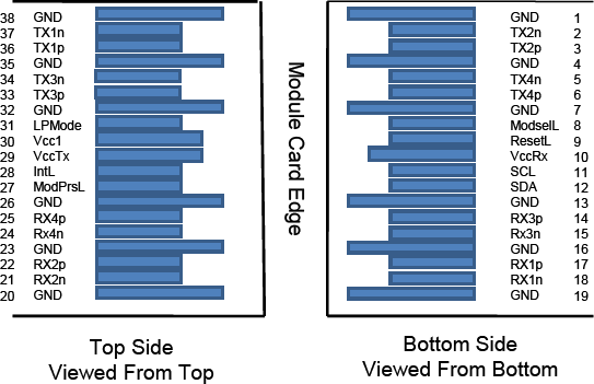
Pin Definitions
|
Pin |
Logic |
Symbol |
Description |
Plug Sequence |
Notes |
|
1 |
GND |
Ground |
1 |
1 |
|
|
2 |
CML-I |
Tx2n |
Transmitter Inverted Data Input |
3 |
|
|
3 |
CML-I |
Tx2p |
Transmitter Non-Inverted Data Input |
3 |
|
|
4 |
GND |
Ground |
1 |
1 |
|
|
5 |
CML-I |
Tx4n |
Transmitter Inverted Data Input |
3 |
|
|
6 |
CML-I |
Tx4p |
Transmitter Non-Inverted Data Input |
3 |
|
|
7 |
GND |
Ground |
1 |
1 |
|
|
8 |
LVTTL-I |
ModselL |
Module Select |
3 |
|
|
9 |
LVTTL-I |
ResetL |
Module Reset |
3 |
|
|
10 |
Vcc Rx |
+3.3V Power Supply Receiver |
2 |
2 |
|
|
11 |
LVCMOS-I/O |
SCL |
2-wire serial interface clock |
3 |
|
|
12 |
LVCMOS-I/O |
SDA |
2-wire serial interface data |
3 |
|
|
13 |
GND |
Ground |
1 |
1 |
|
|
14 |
CML-O |
Rx3p |
Receiver Non-Inverted Data Output |
3 |
|
|
15 |
CML-O |
Rx3n |
Receiver Inverted Data Output |
3 |
|
|
16 |
GND |
Ground |
1 |
1 |
|
|
17 |
CML-O |
Rx1p |
Receiver Non-Inverted Data Output |
3 |
|
|
18 |
CML-O |
Rx1n |
Receiver Inverted Data Output |
3 |
|
|
19 |
GND |
Ground |
1 |
1 |
|
|
20 |
GND |
Ground |
1 |
1 |
|
|
21 |
CML-O |
Rx2n |
Receiver Inverted Data Output |
3 |
|
|
22 |
CML-O |
Rx2p |
Receiver Non-Inverted Data Output |
3 |
|
|
23 |
GND |
Ground |
1 |
1 |
|
|
24 |
CML-O |
Rx4n |
Receiver Inverted Data Output |
3 |
|
|
25 |
CML-O |
Rx4p |
Receiver Non-Inverted Data Output |
3 |
|
|
26 |
GND |
Ground |
1 |
1 |
|
|
27 |
LVTTL-O |
ModPrsL |
Module Present |
3 |
|
|
28 |
LVTTL-O |
IntL |
Interrupt |
3 |
|
|
29 |
Vcc Tx |
+3.3V Power supply transmitter |
2 |
2 |
|
|
30 |
Vcc1 |
+3.3V Power supply |
2 |
2 |
|
|
31 |
LVTTL-I |
LPMode |
Low Power Mode |
3 |
|
|
32 |
GND |
Ground |
1 |
1 |
|
|
33 |
CML-I |
Tx3p |
Transmitter Non-Inverted Data Input |
3 |
|
|
34 |
CML-I |
Tx3n |
Transmitter Inverted Data Input |
3 |
|
|
35 |
GND |
Ground |
1 |
1 |
|
|
36 |
CML-I |
Tx1p |
Transmitter Non-Inverted Data Input |
3 |
|
|
37 |
CML-I |
Tx1n |
Transmitter Inverted Data Input |
3 |
|
|
38 |
GND |
Ground |
1 |
1 |
Note 1: GND is the symbol for signal and supply (power) common for the QSFP+ module. All are common within the QSFP+ module and all module voltages are referenced to this potential unless otherwise noted. Connect these directly to the host board signal-common ground plane.
Note 2: Vcc Rx, Vcc1 and Vcc Tx are the receiver and transmitter power supplies and shall be applied concurrently.
QSFP+ Module Pad Layout
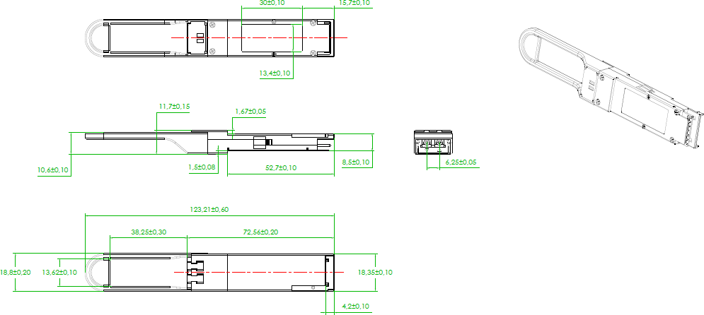
Mechanical Diagram
Warnings
Handling Precautions: This device is susceptible to damage as a result of electrostatic discharge (ESD). A static free environment is highly recommended. Follow guidelines according to proper ESD procedures.
Laser Safety: Radiation emitted by laser devices can be dangerous to human eyes. Avoid eye exposure to direct or indirect radiation.
